17.1 17.2 What Shall We Do? • Let's design a simple processor to understand the entire flow from writing software to Unit 18 designing the hardware – This may not be the most advanced processor but the goal is to give you a fully working example Processor Organization from software to hardware 17.3 17.4 The Instruction Set (1) 
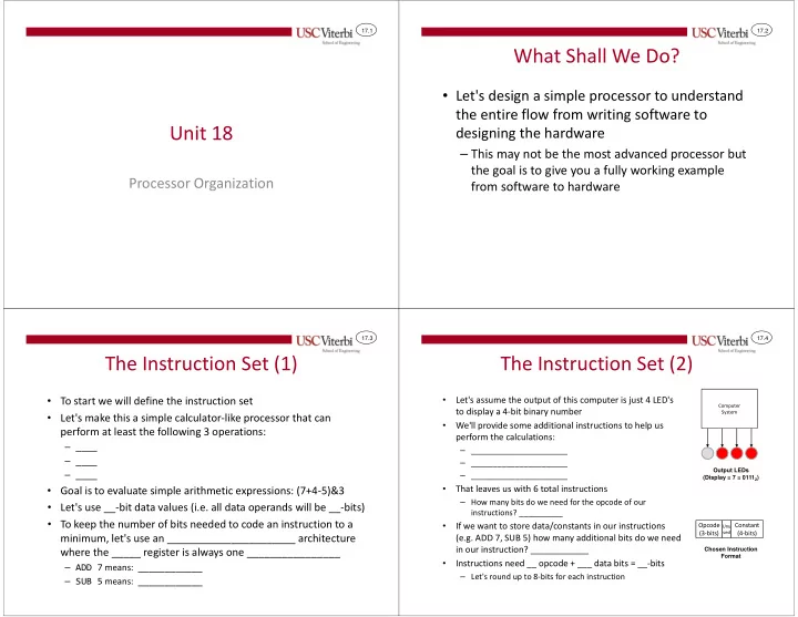
The Instruction Set (2) • Let's assume the output of this computer is just 4 LED's • To start we will define the instruction set Computer to display a 4-bit binary number System • Let's make this a simple calculator-like processor that can • We'll provide some additional instructions to help us perform at least the following 3 operations: perform the calculations: – ____ – ______________________ – ____ – ______________________ Output LEDs – ____ – ______________________ (Display = 7 = 0111 2 ) • That leaves us with 6 total instructions • Goal is to evaluate simple arithmetic expressions: (7+4-5)&3 – How many bits do we need for the opcode of our • Let's use __-bit data values (i.e. all data operands will be __-bits) instructions? __________ • To keep the number of bits needed to code an instruction to a • If we want to store data/constants in our instructions Opcode Constant Unu (3-bits) sed (4-bits) minimum, let's use an ______________________ architecture (e.g. ADD 7, SUB 5) how many additional bits do we need in our instruction? ____________ Chosen Instruction where the _____ register is always one ________________ Format • Instructions need __ opcode + ___ data bits = __-bits – ADD 7 means: ____________ – Let's round up to 8-bits for each instruction – SUB 5 means: ____________
17.5 17.6 Compilation Defining the Machine Code • Consider the following "high-level" code Instruction Set Summary • Machine code refers to the ____________ • ADD k (ACC += k) – (7 - 4 + 6) & 3 • SUB k (ACC -= k) representation of each instruction. • AND k (ACC &= k) • "Compile" it to an appropriate instruction • LOAD k (ACC = k) • We first need to define the actual opcodes so sequence (i.e assembly) • CLR (ACC = 0) • OUT (OUT = ACC) – Assembly refers to the human readable syntax we can translate the assembly you wrote on of each instruction the previous slide into binary for the hardware to execute • Before we do that, let's consider the hardware design as this will help us choose appropriate opcodes • Now we need to convert to binary… 17.7 17.8 Arithmetic and Logic Units Blank ALU To Complete F[2:0] Op. F[2:0] Op. 2-to-1, 4-bit wide mux 000 R = X + Y 100 R = X & Y • Let's define and design the ALU that will Ci=________ 001 R = X - Y 101 Unused I0 010 R = X 110 R = 0 X0 Y C0 perform the various operations our computer X1 011 R = Y - X 111 Unused EE109 ALU I1 X2 A0 X3 S A1 4-bit Binary Adder should support plus a few extra… 2-to-1, 4-bit A2 S0 S0 = ______ wide mux A3 S1 S2 2-to-1, 4-bit B0 R0 2-to-1, 4-bit S3 I0 F[2:0] Op./Result wide mux R1 B1 wide mux Y R2 We just made up Y0 B2 I1 R3 000 R = X + Y these code F2 F1 F0 Y1 B3 We will design what is Y2 S assignments and the I0 Y I0 C4 inside this block. 001 R = X - Y Y3 various operations. 0 Y 0 X0 Remember, we 0 I1 I1 S3 = ________ 0 010 R = X definitely need to X1 S S support ADD, SUB, X2 R0 EE109 ALU 011 R = Y - X AND, and CLR (R=0). X0 X3 R1 S2 = ______ S1 = ______ 100 R = X & Y R2 X1 Y0 R3 101 Unused Y1 X2 F0 Y2 110 R = 0 F1 X3 Y3 F2 111 Unused EE109 ALU
17.9 17.10 Control Logic Completed ALU F0 0 1 F2F1 1 00 2-to-1, 4-bit F[2:0] Op. F[2:0] Op. R FS[2:0] S0 S1 S2 Ci S3 01 wide mux 000 R = X + Y 100 R = X & Y Ci=F0 X+Y 000 001 R = X - Y 101 Unused d 11 I0 X0 010 R = X 110 R = 0 Y X-Y 001 C0 d X1 EE109 ALU 10 I1 A0 011 R = Y - X 111 Unused X2 X 010 S2 X3 S A1 4-bit Binary Adder F0 2-to-1, 4-bit A2 S0 Y-X 011 0 1 F2F1 S0 = F1 • F0 wide mux A3 S1 1 00 S2 X & Y 100 2-to-1, 4-bit B0 R0 2-to-1, 4-bit S3 I0 wide mux R1 01 1 B1 wide mux Y unused 101 R2 Y0 B2 I1 R3 d d Y1 11 B3 0 110 Y2 S I0 Y I0 C4 Y3 Y 0 d d 0 10 unused 111 0 I1 S3 = F2 I1 0 Ci S S F0 F0 F0 0 1 0 1 0 1 F2F1 F2F1 F2F1 S1 = F1 • F0' S2 = F1' • F0 X0 • S0 = 00 00 00 • S1 = X1 01 1 01 1 01 • S2 = X2 F0 Ci = • d d 1 d 1 d 11 F1 11 11 X3 F2 • S3 = d d 1 d 10 10 10 EE109 ALU S3 S0 S1 17.11 17.12 Aside: Impacts of Coding (1) Aside: Impacts of Coding (2) F0 0 1 F2F1 1 00 R FS[2:0] S0 S1 S2 Ci S3 01 1 • What if we changed the codes used for each X + Y 000 0 0 0 0 0 d d 11 Y - X 001 1 0 1 1 0 operation? 10 X - Y 010 0 0 1 1 0 F0 0 011 d 1 0 d 1 0 1 F2F1 1 00 X 100 0 1 0 0 0 F[2:0] Op./Result F[2:0] Op./Result 01 1 d We just made up X&Y 101 0 0 0 d 1 000 R = X + Y these code 000 R = X + Y d d assignments and the 11 Unused 110 d d d d d 001 R = X - Y various operations. 001 R = Y - X Remember, we d 10 Unused 111 d d d d d 010 R = X definitely need to 010 R = X - Y support ADD, SUB, 011 R = Y - X AND, and CLR (R=0). 011 R = 0 F0 F0 F0 0 1 0 1 0 1 F2F1 F2F1 F2F1 • S0 = F2'F0 100 R = X & Y 100 R = X 1 00 00 00 • S1 = F2F0' + F1F0 101 Unused 101 R = X&Y 01 d 01 1 01 1 • S2 = F2F0' + F2'F1'F0 110 R = 0 110 Unused • Ci = F1+F0 d d d d d d 11 11 11 111 Unused 111 Unused • S3 = F1F0 + F2F0 1 1 10 10 10 Notice how much more logic this coding yields.
17.13 17.14 Defining the Machine Code Format Assembler • Using the ALU design can you suggest opcodes for the various • Now translate the assembly you Instruc. OPCODE Op./Result instructions? found from a few slides back to ADD 000 ACC = ACC + C – The accumulator (ACC) will be connected to the result of the ALU machine code and show it as 2 hex OUT 001 OUT = ACC – But should the ACC be connected to the X or Y input of the ALU? digits per instruction LOAD 010 ACC = C • Important: We achieve Load by passing __ through the ALU to the ACC, so we need SUB 011 ACC = ACC - C the constant to come in on X (so ______ cannot) • The "high-level" code was AND 100 ACC = ACC & C – (7 - 4 + 6) & 3 F[2:0] Op./Result Instruc. OPCODE Op./Result - 101 Unused • "Compile" it to an appropriate 000 R = X + Y 000 Instruction Set Summary CLR 110 ACC = 0 • ADD k (ACC += k) instruction sequence (i.e assembly) 001 R = X - Y 001 - 111 Unused • SUB k (ACC -= k) 010 R = X 010 – CLR = ______ • AND k (ACC &= k) + = • LOAD k (ACC = k) 011 R = Y - X 011 – ADD 7 = ______ • CLR (ACC = 0) 100 R = X & Y 100 – SUB 4 = ______ • OUT (OUT = ACC) Opcode Constant Unu 101 Unused 101 sed (3-bits) (4-bits) – ADD 6 = ______ 110 R = 0 110 – AND 3 = ______ Chosen Instruction 111 Unused 111 Format 17.15 17.16 Processor Datapath Sample Execution of SUB 11 • Now let's consider the processor data path Control Instruction Fetch Logic Instruction Fetch Logic Instruction Fetch Logic Control Control 5-bit I0 1 D0 0 Counter Q0 A0 I1 1 0 D1 5-bit 5-bit I0 I0 Q1 A1 32x8 I2 0 D0 D0 0 D2 Counter Counter Q0 Q0 A0 A0 I1 I1 I3 Q2 A2 Memory 1 0 D1 D1 0 D3 I5 Q1 Q1 A1 A1 32x8 32x8 I2 I2 I4 Q3 A3 I6 OUT_LD 0 D2 D2 D4 0 I3 I3 I7 Q2 Q2 A2 A2 Memory Memory RESET Q4 A4 I5 D3 D3 1 1 CLR D5 I4 I4 Q3 Q3 A3 A3 I6 CLK I5 D4 D4 CLK D6 1 ACC_LD I6 RESET RESET Q4 Q4 A4 A4 I5 I5 I7 CLR CLR I7 D5 D5 D7 0 or CLK CLK I6 I6 I5 CLK CLK D6 D6 I6 ACC_LD I7 I7 D7 D7 I7 0 1 1 I7 I7 I6 I6 I5 I5 F2 F1 F0 1 F2 F2 F1 F1 F0 F0 X0 1 ACC[3:0] OUT[3:0] OUT[3:0] X1 0 1 0 X0 X0 ACC[3:0] ACC[3:0] OUT[3:0] OUT[3:0] D0 Q0 X2 R0 D0 D0 Q0 Q0 EE109 ALU 1 1 1 X1 X1 X3 R1 D1 Q1 D1 D1 D0 D0 Q0 Q0 0 1 Q1 Q1 X2 X2 R0 R0 D0 D0 Q0 Q0 EE109 ALU EE109 ALU D2 Q2 0 R2 D2 D2 D1 D1 Q1 Q1 X3 X3 R1 R1 D1 D1 0 1 Q1 Q1 Y0 Q2 Q2 D3 Q3 R3 D3 D3 1 D2 D2 Q2 Q2 D2 D2 R2 R2 Y1 Y0 Y0 Q3 Q3 Q2 Q2 1 D3 D3 Q3 Q3 D3 D3 R3 R3 Y2 ACC_LD Y1 Y1 1 OUT_LD OUT_LD EN Q3 Q3 1 EN EN Y3 LEDs Y2 Y2 0 ACC_LD ACC_LD CLK CLK CLK OUT_LD OUT_LD CLK CLK CLK EN EN EN EN Y3 Y3 LEDs LEDs CLK CLK CLK CLK CLK CLK CLK CLK
Recommend
More recommend