Warmup Use a k-map to fi nd a minimal implementation of this truth - - PowerPoint PPT Presentation

warmup
SMART_READER_LITE
LIVE PREVIEW

Warmup Use a k-map to fi nd a minimal implementation of this truth - - PowerPoint PPT Presentation

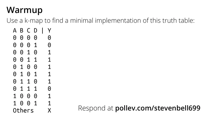
Warmup Use a k-map to fi nd a minimal implementation of this truth table: A B C D | Y 0 0 0 0 0 0 0 0 1 0 0 0 1 0 1 0 0 1 1 1 0 1 0 0 1 0 1 0 1 1 0 1 1 0 1 0 1 1 1 0 1 0 0 0 1 1 0 0 1 1 Respond at pollev.com/stevenbell699


slide-1
SLIDE 1

Warmup

Use a k-map to find a minimal implementation of this truth table:

Respond at pollev.com/stevenbell699 A B C D | Y 0 0 0 0 0 0 0 1 0 0 1 0 1 0 0 1 1 1 0 1 0 0 1 0 1 0 1 1 0 1 1 0 1 0 1 1 1 1 0 0 0 1 1 0 0 1 1 Others X

slide-2
SLIDE 2

EE 201: Multiplexers and timing

Steven Bell 31 January 2019

slide-3
SLIDE 3

By the end of class today, you should be able to:

Draw a logic diagram using a 2N-input multiplexer to implement an N-variable boolean equation Explain what a multiplexer is Given a circuit and timing information about the gates, calculate the contamination delay and propagation delay Explain what glitches are and why they occur Describe the basic structure of an FPGA

slide-4
SLIDE 4

Multiplexers

000 001 010 011 100 101 110 111 A B C

Select one of 2N inputs based on the binary value of N control wires

slide-5
SLIDE 5

A practical example

1 write_enable

storage element

  • utput

value new value

(updates continuously)

slide-6
SLIDE 6

Implementing XOR

00 01 10 11

A B

Vdd

Y=A⊕B

Using a mux as a look-up table (LUT)

slide-7
SLIDE 7

Multiplexer practice 1

Implement this logic equation using 1) discrete gates 2) 8:1 multiplexer 3) 4:1 multiplexer

Y=AB+ABC

slide-8
SLIDE 8

Implement a 2-bit adder with multiplexers

slide-9
SLIDE 9

iCE40UP block diagram

I/O Bank 0 I/O Bank 2 I2C I2C SPI SPI

HFOSC LFOSC

config

DSP

NVCM

Flip‐flop with Enableand Reset Controls Carry Logic 4‐Input Look‐up Table (LUT)

8 Logic Cells = Programmable Logic Block

PLB

RGB I/O RGB I/O RGB I/O I3C I/O I3C I/O

PLL

5 4 Kb DPRAM 5 4 Kb DPRAM 5 4 Kb DPRAM 5 4 Kb DPRAM 5 4 Kb DPRAM 5 4 Kb DPRAM

I/O Bank 1_SPI

config

DSP DSP DSP DSP DSP DSP DSP 256 Kb SPRAM

PWM IP

5 PLB Rows

50 ns Filter 50 ns Filter 50 ns Delay 50 ns Delay

256 Kb SPRAM 256 Kb SPRAM 256 Kb SPRAM

Figure 3.1. iCE40UP5K Device, Top View

Clock stuff

Fixed-function multipliers

Logic "fabric"

Fixed-function I/O modules

Memory

slide-10
SLIDE 10

= Statically defined by configuration program LUT

Carry Logic

Logic Cell

SR EN D Q

DFF Flip‐flop with

  • ptional enable and

set or reset controls Four‐input Look‐Up Table (LUT)

Clock Enable FCOUT FCIN Set/Reset

Shared Block‐Level Controls Programmable Logic Block (PLB) 8 Logic Cells (LCs)

I0 I1 I2 I3 O 1

Figure 3.2. PLB Block Diagram

iCE40UP logic element

slide-11
SLIDE 11

Timing

Depends on lots of things!

= 400 = 15 pF

switching characteristics, VCC = 5 V, TA = 25°C (see Figure 1)

PARAMETER FROM (INPUT) TO (OUTPUT) TEST CONDITIONS SN5404 SN7404 UNIT PARAMETER (INPUT) (OUTPUT) TEST CONDITIONS MIN TYP MAX UNIT tPLH A Y 12 22 ns tPHL A Y RL Ω, CL 8 15 ns

(excerpts from SN74LS04 datasheet)

= 280 = 50 pF

switching characteristics, VCC = 5 V, TA = 25°C (see Figure 1)

PARAMETER FROM (INPUT) TO (OUTPUT) TEST CONDITIONS SN54S04 SN74S04 UNIT PARAMETER (INPUT) (OUTPUT) TEST CONDITIONS MIN TYP MAX UNIT tPLH A Y 3 4.5 ns tPHL A Y RL = 280 Ω, CL = 15 pF 3 5 ns tPLH A Y 4.5 ns tPHL A Y RL Ω, CL 5 ns

slide-12
SLIDE 12

Timing A Y

RL CL

slide-13
SLIDE 13

Timing

Contamination delay: the soonest that the output might change Propagation delay: the maximum time for the output to settle

slide-14
SLIDE 14

Timing practice

slide-15
SLIDE 15

Who cares?

tcd and tpd combine to determine how fast the circuit can run.

slide-16
SLIDE 16

Glitches

slide-17
SLIDE 17
  • 1. Read the book (4.1-4.2) and complete the pre-class quiz

For Tuesday

Quiz is due at 9AM the day of class, so I can review it cp /ee/201/public_html/quizzes/quiz_04.txt ./ provide ee201 q4 quiz_04.txt www.ece.tufts.edu/ee/201/

  • 2. Homework (posted tomorrow) will be due next Thursday (2/7)