SLIDE 1 The Memory Abstraction
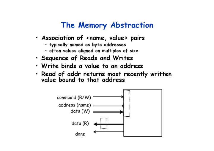
- Association of <name, value> pairs
– typically named as byte addresses – often values aligned on multiples of size
- Sequence of Reads and Writes
- Write binds a value to an address
- Read of addr returns most recently written
value bound to that address
address (name) command (R/W) data (W) data (R) done
SLIDE 2 Relationship of Caches and Pipeline
W B D a t a
A d d e r
I F / I D A L U M e m
y R e g F i l e
M U X
D a t a M e m
y
M U X
Sign Extend
Zero?
M E M / W B E X / M E M
4
A d d e r
Next SEQ PC
RD RD RD
Next PC
A d d r e s s
RS1 RS2 Imm
M U X
I D / E X I-$ D-$ Memory
SLIDE 3 Example: Dual-port vs. Single-port
- Machine A: Dual ported memory
- Machine B: Single ported memory, but its
pipelined implementation has a 1.05 times faster clock rate
- Ideal CPI = 1 for both
- Loads are 40% of instructions executed
– Speedup(enhancement) = Time w/o enhancement / Time w/ – Speedup(B) = Time(A) / Time(B) = CPI(A)xCT(A) / CPI(B)xCT(B) = 1 / (1.4 x 1/1.05) = 0.75
Machine A is 1.33 times faster
SLIDE 4 Memory Hierarchy: Terminology
- Hit: data appears in some block in the upper level
(example: Block X)
– Hit Rate: the fraction of memory access found in the upper level – Hit Time: Time to access the upper level which consists of RAM access time + Time to determine hit/miss
- Miss: data needs to be retrieve from a block in the
lower level (Block Y)
– Miss Rate = 1 - (Hit Rate) – Miss Penalty: Time to replace a block in the upper level + Time to deliver the block the processor
- Hit Time << Miss Penalty (500 instructions on
21264!)
Lower Level Memory Upper Level Memory To Processor From Processor
Blk X Blk Y
SLIDE 5 4 Questions for Memory Hierarchy
- Q1: Where can a block be placed in the upper level?
(Block placement)
- Q2: How is a block found if it is in the upper level?
(Block identification)
- Q3: Which block should be replaced on a miss?
(Block replacement)
- Q4: What happens on a write?
(Write strategy)
SLIDE 6 Simplest Cache: Direct Mapped
Memory 4 Byte Direct Mapped Cache Memory Address
1 2 3 4 5 6 7 8 9 A B C D E F Cache Index 1 2 3
- Location 0 can be occupied by
data from:
– Memory location 0, 4, 8, ... etc. – In general: any memory location whose 2 LSBs of the address are 0s – Address<1:0> => cache index
- Which one should we place in
the cache?
- How can we tell which one is in
the cache?
SLIDE 7 1 KB Direct Mapped Cache, 32B blocks
– The uppermost (32 - N) bits are always the Cache Tag – The lowest M bits are the Byte Select (Block Size = 2 ** M)
Cache Index 1 2 3
:
Cache Data Byte 0 4 31
:
Cache Tag Example: 0x50 Ex: 0x01 0x50
Stored as part
Valid Bit
:
31 Byte 1 Byte 31
:
Byte 32 Byte 33 Byte 63
:
Byte 992 Byte 1023
:
Cache Tag Byte Select Ex: 0x00 9
SLIDE 8 Two-way Set Associative Cache
- N-way set associative: N entries for each Cache
Index
– N direct mapped caches operates in parallel (N typically 2 to 4)
- Example: Two-way set associative cache
– Cache Index selects a “set” from the cache – The two tags in the set are compared in parallel – Data is selected based on the tag result
Cache Data Cache Block 0 Cache Tag Valid
: : :
Cache Data Cache Block 0 Cache Tag Valid
: : :
Cache Index Mux
1 Sel1 Sel0
Cache Block Compare Adr Tag Compare OR Hit
SLIDE 9 Disadvantage of Set Associative Cache
- N-way Set Associative Cache v. Direct Mapped Cache:
– N comparators vs. 1 – Extra MUX delay for the data – Data comes AFTER Hit/Miss
- In a direct mapped cache, Cache Block is available
BEFORE Hit/Miss:
– Possible to assume a hit and continue. Recover later if miss.
Cache Data Cache Block 0 Cache Tag Valid
: : :
Cache Data Cache Block 0 Cache Tag Valid
: : :
Cache Index Mux
1 Sel1 Sel0
Cache Block Compare Adr Tag Compare OR Hit
SLIDE 10 Q1: Where can a block be placed in the upper level?
- Block 12 placed in 8 block cache:
– Fully associative, direct mapped, 2-way set associative – S.A. Mapping = Block Number Modulo Number Sets
Cache
01234567 01234567 01234567
Memory 1111111111222222222233 01234567890123456789012345678901
Full Mapped Direct Mapped (12 mod 8) = 4 2-Way Assoc (12 mod 4) = 0
SLIDE 11 Q2: How is a block found if it is in the upper level?
– No need to check index or block offset
- Increasing associativity shrinks index,
expands tag
Block Offset Block Address Index Tag
SLIDE 12 Q3: Which block should be replaced on a miss?
- Easy for Direct Mapped
- Set Associative or Fully Associative:
– Random – LRU (Least Recently Used)
Assoc: 2-way 4-way 8-way Size LRU Ran LRU Ran LRU Ran 16 KB 5.2% 5.7% 4.7% 5.3% 4.4% 5.0% 64 KB 1.9% 2.0% 1.5% 1.7% 1.4% 1.5% 256 KB 1.15% 1.17% 1.13% 1.13% 1.12% 1.12%
SLIDE 13 Q4: What happens on a write?
- Write through—The information is written
to both the block in the cache and to the block in the lower-level memory.
- Write back—The information is written only
to the block in the cache. The modified cache block is written to main memory only when it is replaced.
– is block clean or dirty?
– WT: read misses cannot result in writes – WB: no repeated writes to same location
- WT always combined with write buffers so
that don’t wait for lower level memory
SLIDE 14 Write Buffer for Write Through
- A Write Buffer is needed between the Cache and
Memory
– Processor: writes data into the cache and the write buffer – Memory controller: write contents of the buffer to memory
- Write buffer is just a FIFO:
– Typical number of entries: 4 – Works fine if: Store frequency (w.r.t. time) << 1 / DRAM write cycle
– Store frequency (w.r.t. time) -> 1 / DRAM write cycle – Write buffer saturation
Processor Cache Write Buffer DRAM
SLIDE 15 A Modern Memory Hierarchy
- By taking advantage of the principle of locality:
– Present the user with as much memory as is available in the cheapest technology. – Provide access at the speed offered by the fastest technology.
Control Datapath Secondary Storage (Disk) Processor Registers Main Memory (DRAM) Second Level Cache (SRAM) On-Chip Cache 1s 10,000,000s (10s ms) Speed (ns): 10s 100s 100s Gs Size (bytes): Ks Ms Tertiary Storage (Disk/Tape) 10,000,000,000s (10s sec) Ts
SLIDE 16 Basic Issues in VM System Design
size of information blocks that are transferred from secondary to main storage (M) block of information brought into M, and M is full, then some region
- f M must be released to make room for the new block -->
replacement policy which region of M is to hold the new block --> placement policy missing item fetched from secondary memory only on the occurrence
- f a fault --> demand load policy
Paging Organization virtual and physical address space partitioned into blocks of equal size page frames pages
pages
reg cache
mem disk frame
SLIDE 17
Address Map
V = {0, 1, . . . , n - 1} virtual address space M = {0, 1, . . . , m - 1} physical address space MAP: V --> M U {0} address mapping function n > m MAP(a) = a' if data at virtual address a is present in physical address a' and a' in M = 0 if data at virtual address a is not present in M Processor Name Space V Addr Trans Mechanism fault handler Main Memory Secondary Memory a a a' missing item fault physical address OS performs this transfer
SLIDE 18 Implications of Virtual Memory for Pipeline design
- Fault?
- Address translation?
SLIDE 19 Paging Organization
frame 0 1 7 1024 7168 P.A. Physical Memory 1K 1K 1K Addr Trans MAP page 0 1 31 1K 1K 1K 1024 31744 unit of mapping also unit of transfer from virtual to physical memory Virtual Memory Address Mapping VA page no. disp 10 Page Table index into page table Page Table Base Reg V
Access Rights
PA
+
table located in physical memory physical memory address actually, concatenation is more likely V.A.
SLIDE 20 Address Translation
- Page table is a large data structure in memory
- Two memory accesses for every load, store, or instruction
fetch!!!
- Virtually addressed cache?
– synonym problem
- Cache the address translations?
CPU Trans- lation Cache Main Memory VA PA miss hit data
SLIDE 21
TLBs
A way to speed up translation is to use a special cache of recently used page table entries -- this has many names, but the most frequently used is Translation Lookaside Buffer or TLB Virtual Address Physical Address Dirty Ref Valid Access Really just a cache on the page table mappings TLB access time comparable to cache access time (much less than main memory access time)
SLIDE 22
Translation Look-Aside Buffers
Just like any other cache, the TLB can be organized as fully associative, set associative, or direct mapped TLBs are usually small, typically not more than 128 - 256 entries even on high end machines. This permits fully associative lookup on these machines. Most mid-range machines use small n-way set associative organizations. CPU TLB Lookup Cache Main Memory VA PA miss hit data Trans- lation hit miss 20 t t 1/2 t Translation with a TLB
SLIDE 23
Reducing Translation Time
Machines with TLBs go one step further to reduce # cycles/cache access They overlap the cache access with the TLB access: high order bits of the VA are used to look in the TLB while low order bits are used as index into cache
SLIDE 24
Overlapped Cache & TLB Access
TLB Cache 10 2 00 4 bytes index 1 K page # disp 20 12 assoc lookup 32 PA Hit/ Miss PA Data Hit/ Miss = IF cache hit AND (cache tag = PA) then deliver data to CPU ELSE IF [cache miss OR (cache tag = PA)] and TLB hit THEN access memory with the PA from the TLB ELSE do standard VA translation
SLIDE 25 Problems With Overlapped TLB Access
Overlapped access only works as long as the address bits used to index into the cache do not change as the result of VA translation This usually limits things to small caches, large page sizes, or high n-way set associative caches if you want a large cache Example: suppose everything the same except that the cache is increased to 8 K bytes instead of 4 K: 11 2 00 virt page # disp 20 12
cache index
This bit is changed by VA translation, but is needed for cache lookup Solutions: go to 8K byte page sizes; go to 2 way set associative cache; or SW guarantee VA[13]=PA[13] 1K 4 4 10 2 way set assoc cache
SLIDE 26 SPEC: System Performance Evaluation Cooperative
– 10 programs yielding a single number (“SPECmarks”)
– SPECInt92 (6 integer programs) and SPECfp92 (14 floating point programs) » Compiler Flags unlimited. March 93 of DEC 4000 Model 610: spice: unix.c:/def=(sysv,has_bcopy,”bcopy(a,b,c)= memcpy(b,a,c)” wave5: /ali=(all,dcom=nat)/ag=a/ur=4/ur=200 nasa7: /norecu/ag=a/ur=4/ur2=200/lc=blas
– new set of programs: SPECint95 (8 integer programs) and SPECfp95 (10 floating point) – “benchmarks useful for 3 years” – Single flag setting for all programs: SPECint_base95, SPECfp_base95
SLIDE 27 SPEC: System Performance Evaluation Cooperative
- Fourth Round 2000: SPEC CPU2000
– 12 Integer – 14 Floating Point – 2 choices on compilation; “aggressive” (SPECint2000,SPECfp2000), “conservative” (SPECint_base2000,SPECfp_base); flags same for all programs, no more than 4 flags, same compiler for conservative, can change for aggressive – multiple data sets so that can train compiler if trying to collect data for input to compiler to improve optimization
SLIDE 28 How to Summarize Performance
- Arithmetic mean (weighted arithmetic mean) tracks
execution time: Σ Σ Σ Σ(Ti)/n or Σ Σ Σ Σ(Wi*Ti)
- Harmonic mean (weighted harmonic mean) of rates (e.g.,
MFLOPS) tracks execution time: n/Σ Σ Σ Σ(1/Ri) or n/Σ Σ Σ Σ(Wi/Ri)
- Normalized execution time is handy for scaling
performance (e.g., X times faster than SPARCstation 10)
- But do not take the arithmetic mean of normalized
execution time, use the geometric mean: ( Π Π Π Π Tj / Nj )1/n
SLIDE 29 SPEC First Round
- One program: 99% of time in single line of code
- New front-end compiler could improve
dramatically
Benchmark 100 200 300 400 500 600 700 800 gcc epresso spice doduc nasa7 li eqntott matrix300 fpppp tomcatv
SLIDE 30 Performance Evaluation
- “For better or worse, benchmarks shape a field”
- Good products created when have:
– Good benchmarks – Good ways to summarize performance
- Given sales is a function in part of performance relative to
competition, investment in improving product as reported by performance summary
- If benchmarks/summary inadequate, then choose between
improving product for real programs vs. improving product to get more sales; Sales almost always wins!
- Execution time is the measure of computer performance!
SLIDE 31 Summary : Caches
- The Principle of Locality:
– Program access a relatively small portion of the address space at any instant of time. » Temporal Locality: Locality in Time » Spatial Locality: Locality in Space
- Three Major Categories of Cache Misses:
– Compulsory Misses: sad facts of life. Example: cold start misses. – Capacity Misses: increase cache size – Conflict Misses: increase cache size and/or associativity.
– Write Through: needs a write buffer. – Write Back: control can be complex
- Today CPU time is a function of (ops, cache misses)
- vs. just f(ops): What does this mean to
Compilers, Data structures, Algorithms?
SLIDE 32 Summary #3/4: The Cache Design Space
- Several interacting dimensions
– cache size – block size – associativity – replacement policy – write-through vs write-back
- The optimal choice is a compromise
– depends on access characteristics » workload » use (I-cache, D-cache, TLB) – depends on technology / cost
Associativity Cache Size Block Size Bad Good Less More
Factor A Factor B
SLIDE 33 Review #4/4: TLB, Virtual Memory
- Caches, TLBs, Virtual Memory all understood by
examining how they deal with 4 questions: 1) Where can block be placed? 2) How is block found? 3) What block is repalced on miss? 4) How are writes handled?
- Page tables map virtual address to physical address
- TLBs make virtual memory practical
– Locality in data => locality in addresses of data, temporal and spatial
- TLB misses are significant in processor performance
– funny times, as most systems can’t access all of 2nd level cache without TLB misses!
- Today VM allows many processes to share single
memory without having to swap all processes to disk; today VM protection is more important than memory hierarchy
SLIDE 34 CPU-DRAM Gap
- 1980: no cache in µproc; 1995 2-level cache on chip
(1989 first Intel µproc with a cache on chip)
Who Cares About the Memory Hierarchy?
µProc 60%/yr. DRAM 7%/yr.
1 10 100 1000
1980 1981 1983 1984 1985 1986 1987 1988 1989 1990 1991 1992 1993 1994 1995 1996 1997 1998 1999 2000
DRAM CPU
1982
Processor-Memory Performance Gap: (grows 50% / year)
Performance
“Moore’s Law” “Less’ Law?”
SLIDE 35 Generations of Microprocessors
- Time of a full cache miss in instructions executed:
1st Alpha: 340 ns/5.0 ns = 68 clks x 2 or 136 2nd Alpha: 266 ns/3.3 ns = 80 clks x 4 or 320 3rd Alpha: 180 ns/1.7 ns =108 clks x 6 or 648
- 1/2X latency x 3X clock rate x 3X Instr/clock ⇒ -5X
SLIDE 36 Processor-Memory Performance Gap “Tax”
Processor % Area %Transistors (-cost) (-power)
37% 77%
61% 94%
64% 88%
– 2 dies per package: Proc/I$/D$ + L2$
- Caches have no “inherent value”,
- nly try to close performance gap
SLIDE 37 What is a cache?
- Small, fast storage used to improve average access
time to slow memory.
- Exploits spacial and temporal locality
- In computer architecture, almost everything is a cache!
– Registers “a cache” on variables – software managed – First-level cache a cache on second-level cache – Second-level cache a cache on memory – Memory a cache on disk (virtual memory) – TLB a cache on page table – Branch-prediction a cache on prediction information? Proc/Regs L1-Cache L2-Cache Memory Disk, Tape, etc. Bigger Faster
SLIDE 38 Traditional Four Questions for Memory Hierarchy Designers
- Q1: Where can a block be placed in the upper level?
(Block placement)
– Fully Associative, Set Associative, Direct Mapped
- Q2: How is a block found if it is in the upper level?
(Block identification)
– Tag/Block
- Q3: Which block should be replaced on a miss?
(Block replacement)
– Random, LRU
- Q4: What happens on a write?
(Write strategy)
– Write Back or Write Through (with Write Buffer)
SLIDE 39
- Miss-oriented Approach to Memory Access:
– CPIExecution includes ALU and Memory instructions CycleTime y MissPenalt MissRate Inst MemAccess Execution CPI IC CPUtime × × × × × × × × × × × × + + + + × × × × = = = = CycleTime y MissPenalt Inst MemMisses Execution CPI IC CPUtime × × × × × × × × + + + + × × × × = = = =
Review: Cache performance
- Separating out Memory component entirely
– AMAT = Average Memory Access Time – CPIALUOps does not include memory instructions CycleTime AMAT Inst MemAccess CPI Inst AluOps IC CPUtime
AluOps
× × × × × × × × + + + + × × × × × × × × = = = = y MissPenalt MissRate HitTime AMAT × × × × + + + + = = = =
( ( ( ( ) ) ) ) ( ( ( ( ) ) ) )
Data Data Data Inst Inst Inst
y MissPenalt MissRate HitTime y MissPenalt MissRate HitTime × × × × + + + + + + + + × × × × + + + + = = = =
SLIDE 40 Impact on Performance
- Suppose a processor executes at
– Clock Rate = 200 MHz (5 ns per cycle), Ideal (no misses) CPI = 1.1 – 50% arith/logic, 30% ld/st, 20% control
- Suppose that 10% of memory operations get 50 cycle
miss penalty
- Suppose that 1% of instructions get same miss penalty
- CPI = ideal CPI + average stalls per instruction
1.1(cycles/ins) + [ 0.30 (DataMops/ins) x 0.10 (miss/DataMop) x 50 (cycle/miss)] + [ 1 (InstMop/ins) x 0.01 (miss/InstMop) x 50 (cycle/miss)] = (1.1 + 1.5 + .5) cycle/ins = 3.1
- 58% of the time the proc is stalled waiting for memory!
- AMAT=(1/1.3)x[1+0.01x50]+(0.3/1.3)x[1+0.1x50]=2.54
SLIDE 41 Unified vs Split Caches
- Unified vs Separate I&D
- Example:
– 16KB I&D: Inst miss rate=0.64%, Data miss rate=6.47% – 32KB unified: Aggregate miss rate=1.99%
- Which is better (ignore L2 cache)?
– Assume 33% data ops ⇒ 75% accesses from instructions (1.0/1.33) – hit time=1, miss time=50 – Note that data hit has 1 stall for unified cache (only one port)
AMATHarvard=75%x(1+0.64%x50)+25%x(1+6.47%x50) = 2.05 AMATUnified=75%x(1+1.99%x50)+25%x(1+1+1.99%x50)= 2.24
Proc I-Cache-1 Proc Unified Cache-1 Unified Cache-2 D-Cache-1 Proc Unified Cache-2
SLIDE 42 How to Improve Cache Performance?
- 1. Reduce the miss rate,
- 2. Reduce the miss penalty, or
- 3. Reduce the time to hit in the cache.
y MissPenalt MissRate HitTime AMAT × × × × + + + + = = = =
SLIDE 43 Where to misses come from?
– Compulsory—The first access to a block is not in the cache,
so the block must be brought into the cache. Also called cold start misses or first reference misses. (Misses in even an Infinite Cache)
– Capacity—If the cache cannot contain all the blocks needed
during execution of a program, capacity misses will occur due to blocks being discarded and later retrieved. (Misses in Fully Associative Size X Cache)
– Conflict—If block-placement strategy is set associative or
direct mapped, conflict misses (in addition to compulsory & capacity misses) will occur because a block can be discarded and later retrieved if too many blocks map to its set. Also called collision misses or interference misses. (Misses in N-way Associative, Size X Cache)
– Coherence - Misses caused by cache coherence.
SLIDE 44
Cache Size (KB) 0.02 0.04 0.06 0.08 0.1 0.12 0.14 1 2 4 8 16 32 64 128 1-way 2-way 4-way 8-way Capacity Compulsory
3Cs Absolute Miss Rate (SPEC92)
Conflict
SLIDE 45 Cache Size
- Old rule of thumb: 2x size => 25% cut in miss rate
- What does it reduce?
Cache Size (KB) 0.02 0.04 0.06 0.08 0.1 0.12 0.14 1 2 4 8 16 32 64 128 1-way 2-way 4-way 8-way Capacity Compulsory
SLIDE 46 Cache Organization?
- Assume total cache size not changed:
- What happens if:
1) Change Block Size: 2) Change Associativity: 3) Change Compiler: Which of 3Cs is obviously affected?
SLIDE 47
Block Size (bytes) Miss Rate 0% 5% 10% 15% 20% 25% 16 32 64 128 256 1K 4K 16K 64K 256K
Larger Block Size (fixed size&assoc)
Reduced compulsory misses Increased Conflict Misses
What else drives up block size?
SLIDE 48
Cache Size (KB) 0.02 0.04 0.06 0.08 0.1 0.12 0.14 1 2 4 8 16 32 64 128 1-way 2-way 4-way 8-way Capacity Compulsory
Associativity
Conflict
SLIDE 49
3Cs Relative Miss Rate
Cache Size (KB) 0% 20% 40% 60% 80% 100% 1 2 4 8 16 32 64 128 1-way 2-way 4-way 8-way Capacity Compulsory
Conflict
Flaws: for fixed block size Good: insight => invention
SLIDE 50 Associativity vs Cycle Time
- Beware: Execution time is only final measure!
- Why is cycle time tied to hit time?
- Will Clock Cycle time increase?
– Hill [1988] suggested hit time for 2-way vs. 1-way external cache +10%, internal + 2% – suggested big and dumb caches
Effective cycle time of assoc pzrbski ISCA
SLIDE 51 Example: Avg. Memory Access Time
- vs. Miss Rate
- Example: assume CCT = 1.10 for 2-way, 1.12 for
4-way, 1.14 for 8-way vs. CCT direct mapped
Cache Size Associativity (KB) 1-way 2-way 4-way 8-way 1 2.33 2.15 2.07 2.01 2 1.98 1.86 1.76 1.68 4 1.72 1.67 1.61 1.53 8 1.46 1.48 1.47 1.43 16 1.29 1.32 1.32 1.32 32 1.20 1.24 1.25 1.27 64 1.14 1.20 1.21 1.23 128 1.10 1.17 1.18 1.20 (Red means A.M.A.T. not improved by more associativity)
SLIDE 52 Fast Hit Time + Low Conflict => Victim Cache
- How to combine fast hit time
- f direct mapped
yet still avoid conflict misses?
discarded from cache
- Jouppi [1990]: 4-entry victim
cache removed 20% to 95% of conflicts for a 4 KB direct mapped data cache
- Used in Alpha, HP machines
To Next Lower Level In Hierarchy
DATA
TAGS One Cache line of Data
Tag and Comparator
One Cache line of Data
Tag and Comparator
One Cache line of Data
Tag and Comparator
One Cache line of Data
Tag and Comparator
SLIDE 53 Reducing Misses via “Pseudo-Associativity”
- How to combine fast hit time of Direct Mapped and have the
lower conflict misses of 2-way SA cache?
- Divide cache: on a miss, check other half of cache to see if
there, if so have a pseudo-hit (slow hit)
- Drawback: CPU pipeline is hard if hit takes 1 or 2 cycles
– Better for caches not tied directly to processor (L2) – Used in MIPS R1000 L2 cache, similar in UltraSPARC
Hit Time Pseudo Hit Time Miss Penalty Time
SLIDE 54 Reducing Misses by Hardware Prefetching of Instructions & Data
- E.g., Instruction Prefetching
– Alpha 21064 fetches 2 blocks on a miss – Extra block placed in “stream buffer” – On miss check stream buffer
- Works with data blocks too:
– Jouppi [1990] 1 data stream buffer got 25% misses from 4KB cache; 4 streams got 43% – Palacharla & Kessler [1994] for scientific programs for 8 streams got 50% to 70% of misses from 2 64KB, 4-way set associative caches
- Prefetching relies on having extra memory
bandwidth that can be used without penalty
SLIDE 55 Reducing Misses by Software Prefetching Data
– Load data into register (HP PA-RISC loads) – Cache Prefetch: load into cache (MIPS IV, PowerPC, SPARC v. 9) – Special prefetching instructions cannot cause faults; a form of speculative execution
- Prefetching comes in two flavors:
– Binding prefetch: Requests load directly into register. » Must be correct address and register! – Non-Binding prefetch: Load into cache. » Can be incorrect. Faults?
- Issuing Prefetch Instructions takes time
– Is cost of prefetch issues < savings in reduced misses? – Higher superscalar reduces difficulty of issue bandwidth
SLIDE 56 Reducing Misses by Compiler Optimizations
- McFarling [1989] reduced caches misses by 75%
- n 8KB direct mapped cache, 4 byte blocks in software
- Instructions
– Reorder procedures in memory so as to reduce conflict misses – Profiling to look at conflicts(using tools they developed)
– Merging Arrays: improve spatial locality by single array of compound elements
– Loop Interchange: change nesting of loops to access data in order stored in memory – Loop Fusion: Combine 2 independent loops that have same looping and some variables overlap – Blocking: Improve temporal locality by accessing “blocks” of data repeatedly
- vs. going down whole columns or rows
SLIDE 57
Merging Arrays Example
/* Before: 2 sequential arrays */ int val[SIZE]; int key[SIZE]; /* After: 1 array of stuctures */ struct merge { int val; int key; }; struct merge merged_array[SIZE];
Reducing conflicts between val & key; improve spatial locality
SLIDE 58
Loop Interchange Example
/* Before */ for (k = 0; k < 100; k = k+1) for (j = 0; j < 100; j = j+1) for (i = 0; i < 5000; i = i+1) x[i][j] = 2 * x[i][j]; /* After */ for (k = 0; k < 100; k = k+1) for (i = 0; i < 5000; i = i+1) for (j = 0; j < 100; j = j+1) x[i][j] = 2 * x[i][j];
Sequential accesses instead of striding through memory every 100 words; improved spatial locality
SLIDE 59
Loop Fusion Example
/* Before */ for (i = 0; i < N; i = i+1) for (j = 0; j < N; j = j+1) a[i][j] = 1/b[i][j] * c[i][j]; for (i = 0; i < N; i = i+1) for (j = 0; j < N; j = j+1) d[i][j] = a[i][j] + c[i][j]; /* After */ for (i = 0; i < N; i = i+1) for (j = 0; j < N; j = j+1) { a[i][j] = 1/b[i][j] * c[i][j]; d[i][j] = a[i][j] + c[i][j];}
2 misses per access to a & c vs. one miss per access; improve spatial locality
SLIDE 60 Blocking Example
/* Before */ for (i = 0; i < N; i = i+1) for (j = 0; j < N; j = j+1) {r = 0; for (k = 0; k < N; k = k+1){ r = r + y[i][k]*z[k][j];}; x[i][j] = r; };
– Read all NxN elements of z[] – Read N elements of 1 row of y[] repeatedly – Write N elements of 1 row of x[]
- Capacity Misses a function of N & Cache Size:
– 2N3 + N2 => (assuming no conflict; otherwise …)
- Idea: compute on BxB submatrix that fits
SLIDE 61 Blocking Example
/* After */ for (jj = 0; jj < N; jj = jj+B) for (kk = 0; kk < N; kk = kk+B) for (i = 0; i < N; i = i+1) for (j = jj; j < min(jj+B-1,N); j = j+1) {r = 0; for (k = kk; k < min(kk+B-1,N); k = k+1) { r = r + y[i][k]*z[k][j];}; x[i][j] = x[i][j] + r; };
- B called Blocking Factor
- Capacity Misses from 2N3 + N2 to N3/B+2N2
- Conflict Misses Too?
SLIDE 62 Reducing Conflict Misses by Blocking
- Conflict misses in caches not FA vs. Blocking size
– Lam et al [1991] a blocking factor of 24 had a fifth the misses
- vs. 48 despite both fit in cache
Blocking Factor 0.05 0.1 50 100 150 Fully Associative Cache Direct Mapped Cache
SLIDE 63
Performance Improvement 1 1.5 2 2.5 3 compress cholesky (nasa7) spice mxm (nasa7) btrix (nasa7) tomcatv gmty (nasa7) vpenta (nasa7) merged arrays loop interchange loop fusion blocking
Summary of Compiler Optimizations to Reduce Cache Misses (by hand)
SLIDE 64 Summary: Miss Rate Reduction
- 3 Cs: Compulsory, Capacity, Conflict
- 0. Larger cache
- 1. Reduce Misses via Larger Block Size
- 2. Reduce Misses via Higher Associativity
- 3. Reducing Misses via Victim Cache
- 4. Reducing Misses via Pseudo-Associativity
- 5. Reducing Misses by HW Prefetching Instr, Data
- 6. Reducing Misses by SW Prefetching Data
- 7. Reducing Misses by Compiler Optimizations
- Prefetching comes in two flavors:
– Binding prefetch: Requests load directly into register. » Must be correct address and register! – Non-Binding prefetch: Load into cache. » Can be incorrect. Frees HW/SW to guess!
CPUtime = IC × CPI Execution + Memory accesses Instruction × Miss rate × Miss penalty × Clock cycle time
SLIDE 65 Review: Improving Cache Performance
- 1. Reduce the miss rate,
- 2. Reduce the miss penalty, or
- 3. Reduce the time to hit in the cache.
SLIDE 66 Write Policy: Write-Through vs Write-Back
- Write-through: all writes update cache and underlying
memory/cache
– Can always discard cached data - most up-to-date data is in memory – Cache control bit: only a valid bit
- Write-back: all writes simply update cache
– Can’t just discard cached data - may have to write it back to memory – Cache control bits: both valid and dirty bits
– Write-through: » memory (or other processors) always have latest data » Simpler management of cache – Write-back: » much lower bandwidth, since data often overwritten multiple times » Better tolerance to long-latency memory?
SLIDE 67 Write Policy 2: Write Allocate vs Non-Allocate (What happens on write-miss)
- Write allocate: allocate new cache line in cache
– Usually means that you have to do a “read miss” to fill in rest of the cache-line! – Alternative: per/word valid bits
- Write non-allocate (or “write-around”):
– Simply send write data through to underlying memory/cache - don’t allocate new cache line!
SLIDE 68
- 1. Reducing Miss Penalty:
Read Priority over Write on Miss
write buffer CPU
in out
DRAM (or lower mem) Write Buffer
SLIDE 69
- 1. Reducing Miss Penalty:
Read Priority over Write on Miss
- Write-through w/ write buffers => RAW conflicts
with main memory reads on cache misses
– If simply wait for write buffer to empty, might increase read miss penalty (old MIPS 1000 by 50% ) – Check write buffer contents before read; if no conflicts, let the memory access continue
- Write-back want buffer to hold displaced blocks
– Read miss replacing dirty block – Normal: Write dirty block to memory, and then do the read – Instead copy the dirty block to a write buffer, then do the read, and then do the write – CPU stall less since restarts as soon as do read
SLIDE 70
Early Restart and Critical Word First
- Don’t wait for full block to be loaded before
restarting CPU
– Early restart—As soon as the requested word of the block ar rives, send it to the CPU and let the CPU continue execution – Critical Word First—Request the missed word first from memory and send it to the CPU as soon as it arrives; let the CPU continue execution while filling the rest of the words in the block. Also called wrapped fetch and requested word first
- Generally useful only in large blocks,
- Spatial locality => tend to want next sequential
word, so not clear if benefit by early restart
block
SLIDE 71
- 3. Reduce Miss Penalty: Non-blocking
Caches to reduce stalls on misses
- Non-blocking cache or lockup-free cache allow data
cache to continue to supply cache hits during a miss
– requires F/E bits on registers or out-of-order execution – requires multi-bank memories
- “hit under miss” reduces the effective miss penalty
by working during miss vs. ignoring CPU requests
- “hit under multiple miss” or “miss under miss” may
further lower the effective miss penalty by
- verlapping multiple misses
– Significantly increases the complexity of the cache controller as there can be multiple outstanding memory accesses – Requires muliple memory banks (otherwise cannot support) – Penium Pro allows 4 outstanding memory misses
SLIDE 72 Value of Hit Under Miss for SPEC
- FP programs on average: AMAT= 0.68 -> 0.52 -> 0.34 -> 0.26
- Int programs on average: AMAT= 0.24 -> 0.20 -> 0.19 -> 0.19
- 8 KB Data Cache, Direct Mapped, 32B block, 16 cycle miss
Hit Under i Misses
0.2 0.4 0.6 0.8 1 1.2 1.4 1.6 1.8 2 eqntott espresso xlisp compress mdljsp2 ear fpppp tomcatv swm256 doduc su2cor wave5 mdljdp2 hydro2d alvinn nasa7 spice2g6
0->1 1->2 2->64 Base
Integer Floating Point “Hit under n Misses”
0->1 1->2 2->64 Base
SLIDE 73 4: Add a second-level cache
AMAT = Hit TimeL1 + Miss RateL1 x Miss PenaltyL1 Miss PenaltyL1 = Hit TimeL2 + Miss RateL2 x Miss PenaltyL2 AMAT = Hit TimeL1 + Miss RateL1 x (Hit TimeL2 + Miss RateL2 + Miss PenaltyL2)
– Local miss rate— misses in this cache divided by the total number of memory accesses to this cache (Miss rateL2) – Global miss rate—misses in this cache divided by the total number of memory accesses generated by the CPU – Global Miss Rate is what matters
SLIDE 74 Comparing Local and Global Miss Rates
- 32 KByte 1st level cache;
Increasing 2nd level cache
- Global miss rate close to
single level cache rate provided L2 >> L1
- Don’t use local miss rate
- L2 not tied to CPU clock
cycle!
- Cost & A.M.A.T.
- Generally Fast Hit Times
and fewer misses
- Since hits are few, target
miss reduction
Linear Log Cache Size Cache Size
SLIDE 75 Reducing Misses: Which apply to L2 Cache?
- Reducing Miss Rate
- 1. Reduce Misses via Larger Block Size
- 2. Reduce Conflict Misses via Higher Associativity
- 3. Reducing Conflict Misses via Victim Cache
- 4. Reducing Conflict Misses via Pseudo-Associativity
- 5. Reducing Misses by HW Prefetching Instr, Data
- 6. Reducing Misses by SW Prefetching Data
- 7. Reducing Capacity/Conf. Misses by Compiler Optimizations
SLIDE 76 Relative CPU Time Block Size 1 1.1 1.2 1.3 1.4 1.5 1.6 1.7 1.8 1.9 2 16 32 64 128 256 512 1.36 1.28 1.27 1.34 1.54 1.95
L2 cache block size & A.M.A.T.
- 32KB L1, 8 byte path to memory
SLIDE 77 Reducing Miss Penalty Summary
– Read priority over write on miss – Early Restart and Critical Word First on miss – Non-blocking Caches (Hit under Miss, Miss under Miss) – Second Level Cache
- Can be applied recursively to Multilevel Caches
– Danger is that time to DRAM will grow with multiple levels in between – First attempts at L2 caches can make things worse, since increased worst case is worse CPUtime = IC × CPI Execution + Memory accesses Instruction × Miss rate × Miss penalty × Clock cycle time
SLIDE 78 What is the Impact of What You’ve Learned About Caches?
= ƒ(no. operations)
– Pipelined Execution & Fast Clock Rate – Out-of-Order execution – Superscalar Instruction Issue
ƒ(non-cached memory accesses)
- Superscalar, Out-of-Order machines hide L1 data cache miss
(-5 clocks) but not L2 cache miss (-50 clocks)?
1 10 100 1000 1980 1981 1982 1983 1984 1985 1986 1987 1988 1989 1990 1991 1992 1993 1994 1995 1996 1997 1998 1999 2000 DRAM CPU
SLIDE 79
Cache Optimization Summary
Technique MR MP HT Complexity Larger Block Size + – Higher Associativity + – 1 Victim Caches + 2 Pseudo-Associative Caches + 2 HW Prefetching of Instr/Data + 2 Compiler Controlled Prefetching + 3 Compiler Reduce Misses + Priority to Read Misses + 1 Early Restart & Critical Word 1st + 2 Non-Blocking Caches + 3 Second Level Caches + 2
miss rate miss penalty
SLIDE 80 Main Memory Background
- Random Access Memory (vs. Serial Access Memory)
- Different flavors at different levels
– Physical Makeup (CMOS, DRAM) – Low Level Architectures (FPM,EDO,BEDO,SDRAM)
- Cache uses SRAM: Static Random Access Memory
– No refresh (6 transistors/bit vs. 1 transistor Size: DRAM/SRAM - 4-8, Cost/Cycle time: SRAM/DRAM - 8-16
- Main Memory is DRAM: Dynamic Random Access Memory
– Dynamic since needs to be refreshed periodically (8 ms, 1% time) – Addresses divided into 2 halves (Memory as a 2D matrix): » RAS or Row Access Strobe » CAS or Column Access Strobe
SLIDE 81 Static RAM (SRAM)
- Six transistors in cross connected fashion
– Provides regular AND inverted outputs – Implemented in CMOS process Single Port 6-T SRAM Cell
SLIDE 82 SRAM Read Timing (typical)
- tAA (access time for address): how long it
takes to get stable output after a change in address.
- tACS (access time for chip select): how long it
takes to get stable output after CS is asserted.
- tOE (output enable time): how long it takes for
the three-state output buffers to leave the high- impedance state when OE and CS are both asserted.
SLIDE 83 SRAM Read Timing (typical)
stable stable stable valid valid valid tAA tOZ ≥ tAA tOE tACS tOZ tOE Max(tAA, tACS) tOH
ADDR CS_L OE_L DOUT WE_L = HIGH
SLIDE 84
- SRAM cells exhibit high speed/poor density
- DRAM: simple transistor/capacitor pairs in
high density form
Dynamic RAM
Word Line Bit Line C Sense Amp
. . .
SLIDE 85 Basic DRAM Cell
– Polysilicon-Diffusion Capacitance, Diffused Bitlines
- Problem: Uses a lot of area (< 1Mb)
- You can’t just ride the process curve to
shrink C (discussed later)
(a) Cross-section (b) Layout
Diffused bit line Polysilicon plate M1 word line Capacitor Polysilicon gate Metal word line
SiO2 n+
Field Oxide Inversion layer induced by plate bias
n+ poly poly
SLIDE 86 Advanced DRAM Cells
SLIDE 87 Advanced DRAM Cells
- Trench Cell (Expand DOWN)
Cell Plate Si Capacitor Insulator Storage Node Poly 2nd Field Oxide Refilling Poly Si Substrate
SLIDE 88 DRAM Operations
– Charge bitline HIGH or LOW and set wordline HIGH
– Bit line is precharged to a voltage halfway between HIGH and LOW, and then the word line is set HIGH. – Depending on the charge in the cap, the precharged bitline is pulled slightly higher
– Sense Amp Detects change
- Explains why Cap can’t shrink
– Need to sufficiently drive bitline – Increase density => increase parasitic capacitance
Word Line Bit Line C Sense Amp
. . .
SLIDE 89 DRAM logical organization (4 Mbit)
- Square root of bits per RAS/CAS
Column Decoder Sense Amps & I/O Memory Array (2,048 x 2,048) A0…A10 … 11 D Q Word Line Storage Cell Row Decoder …
SLIDE 90 So, Why do I freaking care?
- By it’s nature, DRAM isn’t built for speed
– Reponse times dependent on capacitive circuit properties which get worse as density increases
- DRAM process isn’t easy to integrate into
CMOS process
– DRAM is off chip – Connectors, wires, etc introduce slowness – IRAM efforts looking to integrating the two
- Memory Architectures are designed to
minimize impact of DRAM latency
– Low Level: Memory chips – High Level memory designs. – You will pay $$$$$$ and then some $$$ for a good memory system.
SLIDE 91 So, Why do I freaking care?
= ƒ(no. operations)
– Pipelined Execution & Fast Clock Rate – Out-of-Order execution – Superscalar Instruction Issue
ƒ(non-cached memory accesses)
– Compilers?,Operating Systems?, Algorithms? Data Structures?
1 10 100 1000 1980 1981 1982 1983 1984 1985 1986 1987 1988 1989 1990 1991 1992 1993 1994 1995 1996 1997 1998 1999 2000 DRAM CPU
SLIDE 92 4 Key DRAM Timing Parameters
- tRAC: minimum time from RAS line falling to
the valid data output.
– Quoted as the speed of a DRAM when buy – A typical 4Mb DRAM tRAC = 60 ns – Speed of DRAM since on purchase sheet?
- tRC: minimum time from the start of one row
access to the start of the next.
– tRC = 110 ns for a 4Mbit DRAM with a tRAC of 60 ns
- tCAC: minimum time from CAS line falling to
valid data output.
– 15 ns for a 4Mbit DRAM with a tRAC of 60 ns
- tPC: minimum time from the start of one
column access to the start of the next.
– 35 ns for a 4Mbit DRAM with a t
SLIDE 93 A D OE_L 256K x 8 DRAM
9 8
WE_L CAS_L RAS_L OE_L A Row Address WE_L Junk Read Access Time Output Enable Delay CAS_L RAS_L Col Address Row Address Junk Col Address D High Z Data Out DRAM Read Cycle Time Early Read Cycle: OE_L asserted before CAS_L Late Read Cycle: OE_L asserted after CAS_L
begins at:
– The assertion of the RAS_L – 2 ways to read: early or late v. CAS
Junk Data Out High Z
DRAM Read Timing
SLIDE 94 DRAM Performance
– perform a row access only every 110 ns (tRC) – perform column access (tCAC) in 15 ns, but time between column accesses is at least 35 ns (tPC). » In practice, external address delays and turning around buses make it 40 to 50 ns
- These times do not include the time to drive
the addresses off the microprocessor nor the memory controller overhead!
SLIDE 95 Admin
- Hand in homework assignment
- New assignment is/will be on the class
website.
SLIDE 96 Fast Page Mode DRAM
- Page: All bits on the same ROW (Spatial
Locality)
– Don’t need to wait for wordline to recharge – Toggle CAS with new column address
SLIDE 97 Extended Data Out (EDO)
- Overlap Data output w/ CAS toggle
– Later brother: Burst EDO (CAS toggle used to get next addr)
SLIDE 98 Synchronous DRAM
– Data output is in bursts w/ each element clocked
PC100: Intel spec to meet 100MHz memory bus designs. Introduced w/ i440BX chipset Write Read
SLIDE 99 RAMBUS (RDRAM)
- Protocol based RAM w/ narrow (16-bit) bus
– High clock rate (400 Mhz), but long latency – Pipelined operation
- Multiple arrays w/ data transferred on both
edges of clock
RAMBUS Bank RDRAM Memory System
SLIDE 100
RDRAM Timing
SLIDE 101 DRAM History
- DRAMs: capacity +60%/yr, cost –30%/yr
– 2.5X cells/area, 1.5X die size in -3 years
- ‘98 DRAM fab line costs $2B
– DRAM only: density, leakage v. speed
- Rely on increasing no. of computers & memory
per computer (60% market)
– SIMM or DIMM is replaceable unit => computers use any generation DRAM
- Commodity, second source industry
=> high volume, low profit, conservative
– Little organization innovation in 20 years – Don’t want to be chip foundries (bad for RDRAM)
- Order of importance: 1) Cost/bit 2) Capacity
– First RAMBUS: 10X BW, +30% cost => little impact
SLIDE 102 Main Memory Organizations
– CPU, Cache, Bus, Memory same width (32 or 64 bits)
– CPU/Mux 1 word; Mux/Cache, Bus, Memory N words (Alpha: 64 bits & 256 bits; UtraSPARC 512)
– CPU, Cache, Bus 1 word: Memory N Modules (4 Modules); example is word interleaved
SLIDE 103 Main Memory Performance
- Timing model (word size is 32 bits)
– 1 to send address, – 6 access time, 1 to send data – Cache Block is 4 words
= 4 x (1+6+1) = 32
= 1 + 6 + 1 = 8
- Interleaved M.P. = 1 + 6 + 4x1 = 11
SLIDE 104 Independent Memory Banks
- Memory banks for independent accesses
- vs. faster sequential accesses
– Multiprocessor – I/O – CPU with Hit under n Misses, Non-blocking Cache
- Superbank: all memory active on one block transfer
(or Bank)
- Bank: portion within a superbank that is word
interleaved (or Subbank)
Superbank Bank
…
Superbank Number Superbank Offset
Bank Number Bank Offset
SLIDE 105 Independent Memory Banks
number banks ≥ ≥ ≥ ≥ number clocks to access word in bank – For sequential accesses, otherwise will return to
- riginal bank before it has next word ready
- Increasing DRAM => fewer chips => less
banks
RIMM’s can have a HOTSPOT (literally)
SLIDE 106 Avoiding Bank Conflicts
int x[256][512]; for (j = 0; j < 512; j = j+1) for (i = 0; i < 256; i = i+1) x[i][j] = 2 * x[i][j];
- Even with 128 banks, since 512 is multiple of 128,
conflict on word accesses
- SW: loop interchange or declaring array not power of
2 (“array padding”)
- HW: Prime number of banks
– bank number = address mod number of banks – address within bank = address / number of words in bank – modulo & divide per memory access with prime no. banks? – address within bank = address mod number words in bank – bank number? easy if 2N words per bank
SLIDE 107
- Chinese Remainder Theorem
As long as two sets of integers ai and bi follow these rules and that ai and aj are co-prime. If i ≠ ≠ ≠ ≠ j, then the integer x has only one solution (unambiguous mapping): – bank number = b0, number of banks = a0 (= 3 in example) – address within bank = b1, number of words in bank = a1 (= 8 in example) – N word address 0 to N-1, prime no. banks, words power of 2
bi = x mod ai,0 ≤ bi < ai, 0 ≤ x < a 0 × a1 × a 2×…
Fast Bank Number
Modulo Interleaved Bank Number: 1 2 1 2 Address within Bank: 1 2 16 8 1 3 4 5 9 1 17 2 6 7 8 18 10 2 3 9 10 11 3 19 11 4 12 13 14 12 4 20 5 15 16 17 21 13 5 6 18 19 20 6 22 14 7 21 22 23 15 7 23
SLIDE 108
DRAMs per PC over Time
Minimum Memory Size DRAM Generation ‘86 ‘89 ‘92 ‘96 ‘99 ‘02 1 Mb 4 Mb 16 Mb 64 Mb 256 Mb 1 Gb 4 MB 8 MB 16 MB 32 MB 64 MB 128 MB 256 MB 32 8 16 4 8 2 4 1 8 2 4 1 8 2
SLIDE 109 Need for Error Correction!
– Failures/time proportional to number of bits! – As DRAM cells shrink, more vulnerable
- Went through period in which failure rate was low enough
without error correction that people didn’t do correction
– DRAM banks too large now – Servers always corrected memory systems
- Basic idea: add redundancy through parity bits
– Simple but wastful version: » Keep three copies of everything, vote to find right value » 200% overhead, so not good! – Common configuration: Random error correction » SEC-DED (single error correct, double error detect) » One example: 64 data bits + 8 parity bits (11% overhead) » Papers up on reading list from last term tell you how to do these types of codes – Really want to handle failures of physical components as well » Organization is multiple DRAMs/SIMM, multiple SIMMs » Want to recover from failed DRAM and failed SIMM! » Requires more redundancy to do this » All major vendors thinking about this in high-end machines
SLIDE 110 Architecture in practice
- (as reported in Microprocessor Report, Vol 13, No. 5)
– Emotion Engine: 6.2 GFLOPS, 75 million polygons per second – Graphics Synthesizer: 2.4 Billion pixels per second – Claim: Toy Story realism brought to games!
SLIDE 111 FLASH Memory
– Presence of charge => “0” – Erase Electrically or UV (EPROM)
– Reads like DRAM (~ns) – Writes like DISK (~ms). Write is a complex operation
SLIDE 112
- Tunneling Magnetic Junction RAM (TMJ-RAM):
– Speed of SRAM, density of DRAM, non-volatile (no refresh) – New field called “Spintronics”: combination of quantum spin and electronics – Same technology used in high-density disk-drives
– Large magnetic “sled” floating on top of lots of little read/write heads – Micromechanical actuators move the sled back and forth over the heads
More esoteric Storage Technologies?
SLIDE 113
Tunneling Magnetic Junction
SLIDE 114 MEMS-based Storage
- Magnetic “sled” floats
- n array of read/write
heads
– Approx 250 Gbit/in2 – Data rates: IBM: 250 MB/s w 1000 heads CMU: 3.1 MB/s w 400 heads
move media around to align it with heads
– Sweep sled ±50µ µ µ µm in < 0.5µ µ µ µs
in the 1-10GB in 10cm2
See Ganger et all: http://www.lcs.ece.cmu.edu/research/MEMS
SLIDE 115 Main Memory Summary
- Wider Memory
- Interleaved Memory: for sequential or
independent accesses
- Avoiding bank conflicts: SW & HW
- DRAM specific optimizations: page mode &
Specialty DRAM
SLIDE 116 Motivation: Who Cares About I/O?
- CPU Performance: 60% per year
- I/O system performance limited by mechanical
delays (disk I/O)
< 10% per year (IO per sec)
- Amdahl's Law: system speed-up limited by the
slowest part!
10% IO & 10x CPU => 5x Performance (lose 50%) 10% IO & 100x CPU => 10x Performance (lose 90%)
Diminishing fraction of time in CPU Diminishing value of faster CPUs
SLIDE 117 Big Picture: Who cares about CPUs?
- Why still important to keep CPUs busy vs. IO
devices ("CPU time"), as CPUs not costly?
– Moore's Law leads to both large, fast CPUs but also to very small, cheap CPUs – 2001 Hypothesis: 600 MHz PC is fast enough for Office Tools? – PC slowdown since fast enough unless games, new apps?
- People care more about about storing information
and communicating information than calculating
– "Information Technology" vs. "Computer Science" – 1960s and 1980s: Computing Revolution – 1990s and 2000s: Information Age
- Next 3 weeks on storage and communication
SLIDE 118 I/O Systems
Processor Cache Memory - I/O Bus Main Memory I/O Controller Disk Disk I/O Controller I/O Controller Graphics Network
interrupts interrupts
SLIDE 119 Storage Technology Drivers
- Driven by the prevailing computing paradigm
– 1950s: migration from batch to on-line processing – 1990s: migration to ubiquitous computing » computers in phones, books, cars, video cameras, … » nationwide fiber optical network with wireless tails
- Effects on storage industry:
– Embedded storage » smaller, cheaper, more reliable, lower power – Data utilities » high capacity, hierarchically managed storage
SLIDE 120 Outline
- Disk Basics
- Disk History
- Disk options in 2000
- Disk fallacies and performance
- FLASH
- Tapes
- RAID
SLIDE 121 Disk Device Terminology
- Several platters, with information recorded magnetically on both
surfaces (usually)
- Actuator moves head (end of arm,1/surface) over track (“seek”),
select surface, wait for sector rotate under head, then read or write
– “Cylinder”: all tracks under heads
- Bits recorded in tracks, which in turn divided into sectors (e.g.,
512 Bytes)
Platter Outer Track Inner Track Sector Actuator Head Arm