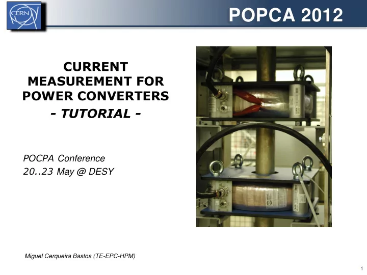
POPCA 2012 CURRENT MEASUREMENT FOR POWER CONVERTERS - TUTORIAL - - - PowerPoint PPT Presentation

popca 2012
SMART_READER_LITE
LIVE PREVIEW

POPCA 2012 CURRENT MEASUREMENT FOR POWER CONVERTERS - TUTORIAL - - - PowerPoint PPT Presentation

POPCA 2012 CURRENT MEASUREMENT FOR POWER CONVERTERS - TUTORIAL - POCPA Conference 20..23 May @ DESY Miguel Cerqueira Bastos (TE-EPC-HPM) 1 CONTENTS Review of current measurement devices Signal transmission Signal conditioning and


slide-1
SLIDE 1

POCPA Conference 20..23 May @ DESY

Miguel Cerqueira Bastos (TE-EPC-HPM)

CURRENT MEASUREMENT FOR POWER CONVERTERS

  • TUTORIAL -

1

POPCA 2012

slide-2
SLIDE 2
  • Review of current measurement devices
  • Signal transmission
  • Signal conditioning and anti-alias filtering
  • Precision components (Voltage references, network resistors and op-amps)
  • ADC choices (SAR/ΔΣ)
  • Temperature coefficient and compensation
  • Powering, PCB layout

CONTENTS

2

Miguel Cerqueira Bastos (TE-EPC-HPM)

slide-3
SLIDE 3

voltage/current signal transmission

CURRENT MEASUREMENT CHAIN

3

Converter Control Current Transducer Power Circuit ADC Anti Aliasing / Signal Conditioning

  • Power converter current loop with digital control
slide-4
SLIDE 4

CURRENT MEASUREMENT TECHNOLOGIES

4

DCCTs Hall effect CTs Rogowsky Shunts Principle

Zero flux detection Hall effect Faraday’s law Faraday’s law Ohm’s law

Output

Voltage or current Voltage or current Voltage Voltage Voltage

Accuracy

Best devices can reach a few ppm stability and repeatability Best devices can reach 0.1% Typically not better than 1% Typically %, better possible with digital integrators Can reach a few ppm for low currents, <% for high currents

Ranges

50A to 20kA hundreds mA to tens

  • f kA

50A to 20kA high currents possible, up to 100kA From <mA up to to several kA

Bandwidth

DC ..kHz for the higher currents, DC..100kHz for lower currents DC up to couple hundred kHz Typically 50Hz up to a few hudreds of kHz Few Hz possible, up to the MHz Up to some hundreds of kHz with coaxial assemblies

Isolation

Yes Yes Yes Yes No

Error sources

Magnetic (remanence, external fields, centering) Burden resistor (thermal settling, stability, linearity, tempco) Output amplifier (stability, noise, CMR, tempco) Magnetic Burden resistor Output amplifier Hall sensor stability (tempco, piezoelectric effect) Magnetic (remanence, external fields, centering, magnetizing current) Burden resistor Magnetic Integrator (offset stability, linearity, tempco) Power coefficient, tempco, ageing, thermal voltages

slide-5
SLIDE 5

voltage/current signal transmission

SIGNAL TRANSMISSION

5

Converter Control Current Transducer Power Circuit ADC Anti Aliasing / Signal Conditioning

slide-6
SLIDE 6

SIGNAL TRANSMISSION

6

Methods of noise coupling:

  • Conductive coupling
  • Common impedance coupling
  • Capacitive and inductive coupling

The main aspects to be considered in a mitigation strategy are:

  • Grounding
  • Cabling and shielding
  • Circuit impedance level
  • Isolation, filtering, balancing

Noise Source Coupling Channel Receptor (DCCT, cable,

  • acq. electronics)
slide-7
SLIDE 7

First Rule: Equipotentiality of reference GND ! (in frequency as well as in DC)

  • Electronic chassis: use conductive surfaces on chassis and ground planes on PCBs
  • Racks – use conductive surfaces and the rack structure for equipotentiality
  • Between racks – ensure “solid”, non inductive ground connections

SIGNAL TRANSMISSION - GROUNDING

7

slide-8
SLIDE 8

Common mode noise

Non perfect grounds often translate into common mode noise problems.

SIGNAL TRANSMISSION – GROUNDING - CM

8

Some well known mitigation methods are:

  • Single ground systems (float source or receiver)
  • Open ground loop (CM chokes, transformers, optos, isolation amplifiers)
  • Common mode filtering
  • Balanced transmission/differential amplifiers
  • Guarded amplifiers

CMV couples into a circuit if grounded at more than

  • ne point. The coupling can happen via a noise current

flowing through a common impedance or by induction of a noise voltage in the ground loop.

slide-9
SLIDE 9

SIGNAL TRANSMISSION – GROUNDING - CM

9

  • Single ground point

ZSG is the isolation impedance If ZSG is high then Ic2 is strongly reduced. Shielding reduces the capacitive nature of ZSG. Often not possible to float the source.

ZSG

  • Common mode chokes

CM currents generate a non cancelling flux in the choke. In practice, due to physical limitations such as limited permeability and number

  • f turns, common mode chokes provide
  • nly moderate attenuation to CM noise.
slide-10
SLIDE 10
  • CM filtering

Attenuation of HF common mode at frequencies where the receiver amplifier circuit has limited or no common mode rejection. Passive filters (LC

  • r

RC) are commonly used. An example of an RF filter for an instrumentation amplifier is shown below.

10

SIGNAL TRANSMISSION – GROUNDING – CM

  • Guarded amplifiers

The guard shield works in conjunction with a floating receiver and a shielded cable to reduce capacitive coupled common mode noise. Without the guard, CM noise would flow from A back to B through R1 and R2.

slide-11
SLIDE 11

SIGNAL TRANSMISSION – GROUNDING - CM

11

  • Differential/balanced inputs

Different types of differential input circuits can be used:

Difference amplifier Instrumentation amplifier Fully differential amplifier Circuit Input impedance

kΩ range – depends on gain resistors, which can’t be too high to limit noise High – corresponds to the input impedance of the buffer amplifiers kΩ range – depends on the gain resistors, which can’t be too high to limit noise

CMR

Depends on matching between gain resistor ratios ! Matched networks often used High, at least in the case of integrated instrumentation amplifiers Depends on matching between gain resistor ratios ! Matched networks often used

ADC signal conditioning

Easy level adapting for ADC inputs Easy level adapting for ADC inputs Well suited for driving differential ADC inputs and transmission lines. Easy level adapting and anti alias filtering

Other

  • Needs return path for the bias

current in case of floating source.

slide-12
SLIDE 12
  • Coaxial vs Shielded twisted pair

STP: preferred below 100kHz. Shield is not a signal conductor. Coaxial: more uniform characteristic impedance, lower losses. Shield is part of signal path, so noise currents should not

SIGNAL TRANSMISSION – CABLING

12

be allowed to flow. For high frequencies, skin effect makes it behave like a triax.

  • Where and how should shields be grounded ? The answer depends on:
  • Type of cable (Coaxial or STP)
  • Frequency range of the transmitted signal and noise voltages
  • Nature of the noise coupling (capacitive or magnetic?)
  • Circuit impedances (source and receiver floating or grounded?)
slide-13
SLIDE 13
  • A grounded shield protects against capacitive coupling. If large CMVs are

present a shield grounded on both sides will conduct a noise current that can couple with the inner conductors.

  • Copper shields provide no magnetic shielding. The best way to shield against

magnetic coupling is to reduce the surface of the signal loop -> twisted pair cables. Use coaxial for frequencies where the signal current returns via the shield and not through ground (f > 5 fshield_cutoff).

  • In low level systems grounded at both ends where magnetic fields are present,

the surface of the ground loop (LO to GND) must also be minimized.

SIGNAL TRANSMISSION – CABLING - SHIELDING

13

slide-14
SLIDE 14

Shielded twisted pair

  • Where power frequency common mode voltages

are present, and the signal being transmitted is a low level, low frequency voltage signal, the shield should be grounded on one side only (receiver end).

  • If either the source or the load are floating the shield

should be grounded at one side only as shown in A and B (except for the case of a guard shield).

  • For all other cases, shields should be grounded on

both sides (E). Coaxial cable

  • If either the source or the load are floating the shield

should only be grounded at one side only (C,D).

  • For all other cases, shields should be grounded on

both sides (F).

SIGNAL TRANSMISSION – CABLING - SHIELDING

14

slide-15
SLIDE 15

Example reflecting some of the concepts discussed before (Single ground, type of cable, shielding):

SIGNAL TRANSMISSION – CABLING - SHIELDING

15

slide-16
SLIDE 16
  • Current transducer output – remote sensing ?

SIGNAL TRANSMISSION – CIRCUIT IMPEDANCE

16

  • DCCT outputs are often available in 4 wire for remote sensing.

+ Eliminates error due to voltage drop in the cable

  • Gain of the differential amplifier becomes dependent of cable impedance
  • A two wire transmission with a high impedance differential input at the

receiver end gives good results. The differential input provides the required CMR.

Op Amp

Precision Amplifier

Burden Resistor

Output Voltage

Is

Hi Sense

Hi

Lo Sense

Lo

Rcable Rcable Op Amp

Precision Amplifier

Burden Resistor

Output Voltage

Is

Hi Sense

Hi

Lo Sense

Lo

slide-17
SLIDE 17

voltage/current signal transmission

SIGNAL CONDITIONING

17

Converter Control Current Transducer Power Circuit ADC Anti Aliasing / Signal Conditioning

slide-18
SLIDE 18
  • The functions to be performed by the signal conditioning circuits derive

from the nature of both the signal and the receiver and may comprise:

  • Current to voltage conversion

(not covered here)

  • Filtering: CM and series

(discussed in previous section)

  • Multiplexing/switching
  • Buffering/ impedance adapting
  • Differential input
  • Level adaptation
  • Anti Alias filtering

SIGNAL CONDITIONING

18

slide-19
SLIDE 19

SIGNAL CONDITIONING

19

multiplexing switching buffering Differential inputs And level adapting filtering filtering

slide-20
SLIDE 20

SIGNAL CONDITIONING

20

Multiplexing/switching Use high impedance inputs to eliminate errors due to mux’s ON resistance. Cross talk and settling time might occur due to source impedance combined with mux’s stray capacitance. Low source impedance also minimizes effect

  • f

charge injection from the multiplexer. Buffering/ impedance adapting ZSource and Zreceiver form voltage

  • divider. Buffering ensures Zreceiver is

large, maximizing the voltage signal at the receiver input. Buffers are used in combination with differential amplifiers to create balanced inputs. Unity gain amplifiers are sensitive to capacitive loads – particular important if dynamics is an issue Level adapting Attenuation or amplification of a voltage signal using voltage dividers and op amp circuits. Level shifting, in particular for ADCs with differential inputs. On fully diff amplifiers the Vocm pin allows the output CMV to be adjusted for precision level shifting.

  • 10V..10V

signal 2.5V ± 1V signal

slide-21
SLIDE 21

21

ANTI-ALIAS FILTERING/ SAMPLING STRATEGIES

The anti-alias requirements/strategy depend on the sampling strategy:

  • Nyquist-Shannon sampling:

fsampling > 2.fmax.signal The anti-alias filter must provide appropriate attenuation above Fmax. Cutoff frequency and filter order depend on desired dynamic range. Below we can see the effect of aliasing on dynamic range. On the right we see the response of a 10th order anti alias filter designed to achieve 60dB dynamic of range for a 3kHz signal bandwidth and 12kSPS sampling speed.

alias free alias limits dynamic range

slide-22
SLIDE 22

22

ANTI-ALIAS FILTERING/ SAMPLING STRATEGIES

  • Oversampling and decimation

fsampling >>> fNyquist Input analogue anti-alias filter significantly

  • relaxed. The filter roll off needs to guarantee

the dynamic range for (k.fs)/2 instead of fs/2. Signal is subsequently digitally filtered and decimated down to the band of interest. Digital low pass has to provide anti alias for fs/2 to guarantee the decimation process is alias free.

  • Synchronized sampling

In PC applications with well known ripple noise, such as PWM converters, aliasing can be used to achieve ripple elimination. In this case, Shannon’s theorem is not respected but used for our advantage. If sampling and switching are perfectly synchronised, the effect of aliasing will be the reconstruction of the average value of the sampled signal, eliminating the ripple.

Reconstructed signal Load current (Sampled signal) Load voltage Ts

slide-23
SLIDE 23

23

ANTI ALIAS FILTERS

  • One pole passive filters are still used where impedance does not impact the

conversion process like at input of DS converters. Otherwise active filters are preferred as they provide isolation and low output impedance. A commonly used circuit is the non inverting second order Sallen-Key filter. Another popular circuit is the inverting double pole multiple feedback shown below. Cascading several stages allows higher order filtering.

Double pole multiple feedback

slide-24
SLIDE 24

24

PRECISION COMPONENTS – VOLTAGE REFERENCES

  • Main technologies:
  • Bandgap: Temperature compensated. Low cost, medium accuracy applications.
  • Buried Zener: Very good long-term stability and low noise. High accuracy applications, higher cost.

Both types can include additional on-chip circuitry to further minimize temperature drift.

  • Important specification parameters
  • Initial error: importance of this parameter depends on calibration strategy
  • Temperature coefficient: auxiliary circuits might be included in the reference for better TC
  • Thermal hysteresis: change in output voltage after temperature cycling. Function of packaging,

IC layout. Can often be improved by a burn in process.

  • Noise: Includes broadband thermal noise and 1/f noise.
  • Long term drift: can be improved by a burn in process which normally involves several days

power cycling at Tambient>80ºC.

  • Line and load regulation
slide-25
SLIDE 25
  • Voltage references
  • Examples – ultra precision voltage reference with buried zener LTZ1000 and precision reference

circuit with the LT1236, using precision network resistors to generate multiple reference voltages.

25

PRECISION COMPONENTS – VOLTAGE REFERENCES

Temperature control using Internal heater Zener current control Temperature sensing (Q2) 10V ref generation 2.5V and 1.25V generation

  • used for voltage

level shifting

slide-26
SLIDE 26

26

PRECISION COMPONENTS - RESISTORS

  • Network resistors
  • For voltage division or amplification, precise ratio devices are now readily
  • found. TCR tracking is of most importance for resistors used as ratio devices
  • Metal foil reaches best accuracies, followed by thin film
  • Tolerance ≠ Precision (a 0.05% thin film will eventually drift to 1% and

prove worse than a 0.5% metal foil which has much better stability).

  • Power coefficient – change due to self heating (TC: changes due to

ambient temperature). In an amplifier configuration with gain > 1 the power PR2 > PR1 which means gain resistor internal heating will be different. Minimizing absolute TC (linked to PC) is therefore also an important factor.

  • Load life stability – mechanical effect of stress relaxation of the resistive

element’s internal construction, normally hundreds/thousands of hours.

  • Thermal and current noise
slide-27
SLIDE 27

27

PRECISION COMPONENTS – OPAMPS

  • Amplifier loading can affect output accuracy,
  • utput swing and stability.
  • Of particular interest for low level high

precision applications are zero drift amplifiers:

  • Chopper stabilized amplifiers

Modulation/demodulation technique (e.g. LTC1052). Normally requires bandwidth limitation to exclude chopper noise

  • Auto zero amplifiers

Uses switched capacitors to store and null the offset (eg AD8638)

  • Important specification parameters
  • Input impedance
  • Input Offset Voltage and offset TC

Particularly important with high CL loop gain

  • Input Bias Current, input noise current

Particularly important in applications with high value gain resistors

  • Open Loop Gain

Defines the feedback loop error

  • Opamp noise

(1/f) at low frequency and white at other frequencies

  • PSRR and CMRR
  • Gain Bandwidth product

Too much bandwidth is not an advantage. Limiting the bandwidth by using a capacitor in parallel with the gain resistor is common practice.

  • Technologies: Bipolar, BiFET, CMOS
slide-28
SLIDE 28

voltage/current signal transmission

ANALOGUE TO DIGITAL CONVERTERS

28

Converter Control Current Transducer Power Circuit ADC Anti Aliasing / Signal Conditioning

slide-29
SLIDE 29

29

ANALOGUE TO DIGITAL CONVERTERS

  • Choice of ADC architecture
  • Criteria: precision, resolution, dynamic range, speed
  • Successive Approximation Register (SAR) converters typically range from 8 to 18

bits with sample speeds up to several MSPS. They have the ability to be connected to multiplexed inputs at a high data acquisition rate.

  • Delta-sigma converters (ΔΣ) have virtually replaced the integrating-type ADCs (e.g.

dual-slope) for applications requiring high resolution (16 bits to 24 bits) and low speed. They are inherently linear and monotonic.

slide-30
SLIDE 30

30

ANALOGUE TO DIGITAL CONVERTERS

  • Delta Sigma – Oversampling, noise shaping, digital filtering and decimation
  • Figure A shows the noise spectrum for a “Nyquist” ADC sampling at fs. Figure B shows how
  • versampling at a K.fs (k = oversampling ratio) spreads the noise energy over a wider frequency
  • range. Figure C shows the effect of the DS integrator in shaping the noise. This shaping can be

exploited to remove most of the noise using a digital filter.

  • The resolution that can be obtained with a DS depends on the oversampling ratio, noise shaping

and the digital filter. On designing the digital filter, a tradeoff between bandwidth and resolution has to be done.

  • Because of oversampling and latency, sigma-delta converters are not often used in multiplexed signal

applications.

  • Idle tones can be a problem in DS ADCs: Tones are caused whenever the modulator output sequence

falls into a cyclic mode. They depend on the modulator (dc) input signal and the initial conditions of the integrator outputs.

slide-31
SLIDE 31

31

TEMPERATURE COEFFICIENT

  • Temperature related errors (TC, thermal voltages) can be minimized by:
  • Choosing components with minimum TC
  • Using cancelling and compensation techniques (ratio devices, diff sensing)
  • Minimizing temperature variations and gradients
  • Temperature control – choice of control range very important: testing as close as

possible to field conditions.

  • Peltier
  • Resistive element
  • Thermal isolation – isolation box, cover, pcb slots
slide-32
SLIDE 32

32

TEMPERATURE COEFFICIENT

  • Temperature related errors (TC, thermal voltages) can be minimized by:
  • Using compensation algorithms
  • First order vs second order – the TC can vary with temperature so a linear

compensation might not be enough

  • Individual vs standard TCs

It might not be possible to use individual TC values for the elements to be compensated, so an average TC might be used as long as the TC spread is not too important.

slide-33
SLIDE 33

33

POWERING AND PCB DESIGN

  • Prefer linear power supplies over switching !
  • If not possible, filter, regulate
  • Power supply decoupling – keep PS impedance <1Ω across frequency

Due to track inductance, local decoupling is necessary:

  • At the PCB entry level + at the IC level
  • Should be done with short, non-inductive connections to gnd
  • Low ESD required, might need paralleling capacitors

Local decoupling also reduces the area of supply current loops.

  • Only gnd planes provide proper reference and shielding
  • Circuit location in the pcb is important, think of return currents – vias and slots

increase inductance

  • Circuit segregation can solve noise and thermal problems. If proper segregation is

achieved, gnd plane splitting is not necessary.

slide-34
SLIDE 34

Publications Spreadbury, Peter J. “The Ultra-Zener–A Portable Replacement for the Weston Cell?” by IEEE Transactions on Instrumentation and Measurement, Vol. 40, No. 2, April 1991, pp. 343-346 Application notes Understanding interference – type noise; Alan Rich, Analog Dialogue 16-3 1982 Shielding and guarding; Analog Dialogue 17-1 1983 Fundamental signal conditioning; Measurement Computing application note Fundamentals of sampled data systems; Analog Devices application note AN-282 Understanding and Applying Voltage References; Mitchell Lee , Linear technology application note 82 How to Select Resistors for Precision Applications, Yuval Hernik, March 26, 2010 ,Vishay application note Which ADC Architecture Is Right for Your Application?; Walt Kester, Analog Dialogue 39-06, June (2005) Books Noise reduction techniques in electronic systems; Herny W. Ott, Wiley interscience Digital Control in Power Electronics; Simone Buso and Paolo Mattavelli, Morgan & Claypool publishers

BIBLIOGRAPHY

34