Petaflops Simulation and Design of Nanoscale Materials and Devices - - PowerPoint PPT Presentation

petaflops simulation and design of nanoscale materials
SMART_READER_LITE
LIVE PREVIEW

Petaflops Simulation and Design of Nanoscale Materials and Devices - - PowerPoint PPT Presentation

Petaflops Simulation and Design of Nanoscale Materials and Devices J. Bernholc, Z. Xiao, E. Briggs, W. Lu NC State University, Raleigh, NC 27695-8202 I. RMG petascale, open-source electronic structure code Blue Waters community Portal


slide-1
SLIDE 1

Petaflops Simulation and Design of Nanoscale Materials and Devices

NC STATE UNIVERSITY

I. RMG – petascale, open-source electronic structure code Blue Waters community Portal Part of Sustained Petascale Performance benchmark Version 3: Cuda-managed memory, Volta support, multiple GPUs per node. Quantum transport (NEGF) module

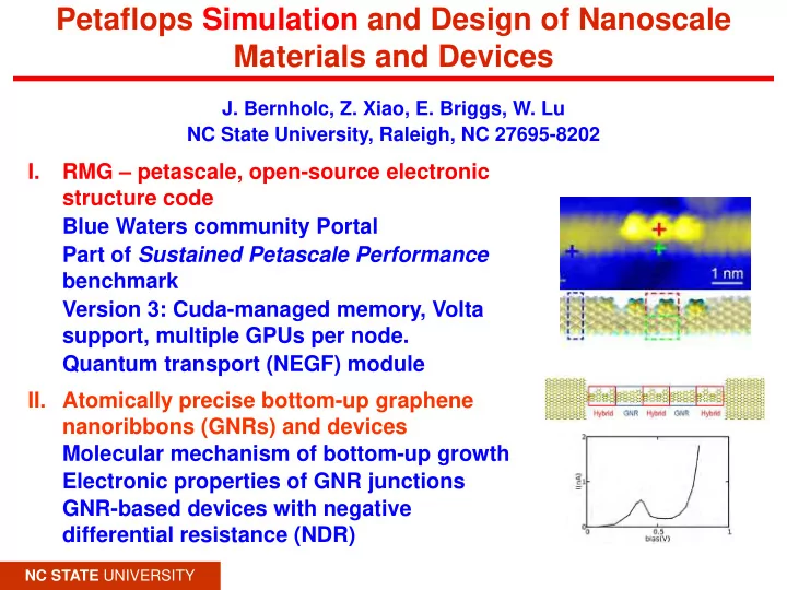
  • II. Atomically precise bottom-up graphene

nanoribbons (GNRs) and devices Molecular mechanism of bottom-up growth Electronic properties of GNR junctions GNR-based devices with negative differential resistance (NDR)

  • J. Bernholc, Z. Xiao, E. Briggs, W. Lu

NC State University, Raleigh, NC 27695-8202

slide-2
SLIDE 2
  • Density functional equations solved directly
  • n the grid
  • Multigrid techniques remove instabilities by

working on one length scale at a time

  • Non-periodic boundary conditions are as

easy as periodic

  • Compact “Mehrstellen” discretization
  • Allows for efficient massively parallel

implementation

Basis Multigrids

Real-space Multi-Grid method (RMG)

] [ ] ) [( ] [

i i i NL eff i

S B V V B A φ ε φ φ = + +

Largest run used 139,392 CPU cores and 8,712 GPU's, > 6.5 PF

Cray XK7

ORNL Amyloid β 1-42 634 atoms

1 node = 16 Opteron cores+ 1 Nvidia K20x GPU

RMG open source

sourceforge.net/projects/rmgdft/ Quantum transport: later in 2017 Performance on 3,872 Cray XK7 (K20x GPU) Blue Water nodes: 1.14 PFLOPS

> 2,300 downloads

www.rmgdft.org

slide-3
SLIDE 3

RMG v2.x performance with Nvidia GP100 Pascal GPU

 Workstation calculation

  • Dual Xeon E5-2630v2 workstation. Total of 12 CPU cores and 32 GBytes RAM.

Nvidia GP100 Pascal, 16GBytes HBM memory and 5.3 TFLOPS double precision.

Test problem 256 atom copper cell

  • Vanderbilt ultrasoft pseudopotentals with 18 beta functions/atom.

Total of 1536 electronic orbitals. PBE XC functonal.  Execution time dominated by eigensolver and large matrix operations

  • CPU only run required 94.4 seconds/SCF step.
  • CPU/GPU run required 19.7 seconds/SCF step.

A single GPU produces a speedup by a factor of 4.8!

slide-4
SLIDE 4

RMG Version 3.0 (to be released next week)

 Design considerations and goals

  • Restructure build process and improve code maintainability. Focus on

next generation hardware features.

  • Open source release of additional components of RMG.

 Bulk of computational power will come from GPUs

  • Much easier to write clean high performance code for more recent
  • hardware. Parallelizes to ~10k of multi-core CPU/multi-GPU nodes.
  • Version 3.0 switches from explicit buffer management to Cuda-managed

memory.

  • May not run well (or at all) on older hardware. Use 2.x versions
  • n them. Nvidia Pascal and later recommended for Version 3.0.

 Additional components to be released in a couple of months

  • Nearly linearly scaling localized orbital code
  • Electron transport module (Non-equilibrium Green's function formalism).

Release and tutorial at joint Electronic Structure Workshop (ES18) and Penn Conference in Theoretical Chemistry (PCTC18), June 11-14, 2018.

slide-5
SLIDE 5

Bottom-up Synthesis of Graphene Nanoribbons

 Molecular precursor:

  • 10,10’-dibromo-9,9’-

bianthryl(DBBA)

  • Adsorbs on metal surfaces

Au(111)

 Polymerization at 200˚C

  • Debromination: molecular

precursors lose Br

  • Self-assembly: poly-anthrylene

is formed.

 Cyclodehydrogenation at 400˚C

  • Cyclization: poly-anthrylene

forms additional C-C bonds.

  • Dehydrogenation: removal of

hydrogen atoms to form graphene nanoribbons.

  • J. Cai et al. Nature, 2010

3D atomic structure of polymer on Au(111) 3D atomic structure of GNR on Au(111)

experiment simulation STM image of polymer experiment simulation STM image of GNR

5

slide-6
SLIDE 6

 Studying separately:

  • Cyclization
  • Dehydrogenation

 Methods:

  • Density functional theory
  • Van der Walls correction for

interaction between metal substrate and molecule:

  • Vdw-df non-local

functional with PBE exchange correlation

  • Nudged Elastic Band

method:

  • Minimum energy pathway
  • Energy barriers

Polymer to GNR transition

Cyclodehydrogenation Cyclization Dehydrogenation

Proposed intermediate state in periodic model

6

slide-7
SLIDE 7

Substrate effect on conversion to GNR

 Cyclization:

  • DBDA adsorption on substrate

lowers the polymer formation energy and cyclization barrier

  • Energy barrier in vacuum: 2.5 eV
  • Energy barrier on Au: 1.8 eV

 Dehydrogenation:

  • Hydrogen atoms adsorb on Au

surface

  • The product is GNR and adsorbed

H atoms

  • Energy barrier for direct

desorption in vacuum: 2.2 eV

  • Energy barrier for adsorption on

Au: 1.3 eV H desorption into vacuum

Substrate effect:

  • Adsorption of polymer on metal catalyzes the cyclization reaction
  • H desorption onto metal substrate promotes dehydrogenation

reaction by significantly decreasing the energy barrier

H desorption onto substrate

7

Cyclization step on substrate

slide-8
SLIDE 8

 Reaction pathway:

  • H atoms remain on different sides after C-C bond

formation

  • One H atom migrates to an edge site by 1-3 sigmatropic

rearrangement.

  • Two H atoms desorb as H2

 Charge effect:

  • Unstable C-C bond formation in the neutral case.
  • Arenium ion stabilizes the transition state in the 2+

charge.

  • Avoids the high energy barrier of H-atom rotation.

Dehydrogenation step

E(eV) +2e

  • 2e

Step 1 1.0 2.5 2.4 Step 2 2.4 4.0 4.2 Step 3 1.3 3.2 4.2

 Dimer model:

  • Finite oligomer

structure: represents

  • rbital symmetry in the

reaction

  • Vacuum environment:

Allows for a charged system Transition state energy results:

  • C. Ma, Z. Xiao, H. Zhang, L. Liang, J. Huang, W. Lu, B. G. Sumpter, K. Hong, J.

Bernholc, A-P. Li, Nature Communications 8, 14815 (2017)

8

slide-9
SLIDE 9

Nanoscale Device with Negative Differential Resistance

9

Double barriers Quantum dot

Source Drain

Double barrier resonant tunneling device

A: threshold B: resonant tunneling C: current valley Barriers: Large gap → narrow ribbon Quantum dot structure Small gap → wide ribbon → hybrid ribbon

slide-10
SLIDE 10

Electronic structure of the GNR-Hybrid junction

10

 Hybrid has a smaller band gap than GNR  Type-I band alignment

LDOS mapping from experiment and calculations. Band alignment from theory agrees with experiment, except for band gap underestimation due to DFT.

slide-11
SLIDE 11

 7-aGNR, has a large gap, can serve as a barrier.  Hybrid polymer/ribbon has a small gap; can act as a quantum dot.  Sizes of the barrier and of the quantum dot affect the negative differential resistance (NDR).  Quantum transport calculations for a variety of structures to identify promising device structures.

GNR-based devices

slide-12
SLIDE 12

µL

E1 E2 LUMO HOMO

µR

GNR-Hybrid-GNR Device

Barriers: two segments of 7-aGNR, length of 8.5 Å Quantum dot: hybrid structure, length of 8.5Å

  • Interface levels E1 and E2 are broadened and decay slowly into

both GNR and graphene region

  • The interface states overlap strongly with HOMO and LUMO of

the hybrid structure.

  • The device is too short, 7-aGNR fails to act as a barrier.
  • Direct tunneling between leads occurs.
  • No clear NDR feature for this short device.
slide-13
SLIDE 13

GNR-Hybrid-GNR Device

Bias o

  • f

f 0. 0.0 V V

µL µR

E1 E2 E1 E2

Bias o

  • f

f 0. 0.65 V V

µL µR

E1 E2 E1 E2

Bias o

  • f

f 0. 0.80 V V

µL µR

E1 E2 E1 E2 Barriers: two segments of 7-aGNR, length of 26 Å Quantum dot: hybrid structure, length of 30 Å

  • 7-aGNR is a true potential barrier for both electron and hole transport.
  • NDR appears at 0.65 eV with peak/valley of 1.8.
  • The current at NDR point is too small (<0.01nA) for a real application.
slide-14
SLIDE 14

Designed new multi-segment structure

 Decrease segment length for larger current  Add two more hybrid segments for easier band alignment  5 parts: Hybrid-GNR-Hybrid-GNR-Hybrid

  • GNRs still serve as barriers

 Increase peak/valley ratio (PVR) of current

Hybrid GNR Hybrid GNR Hybrid

14

slide-15
SLIDE 15

I-V Curve and Level Alignment in Multi-Segment Device

Bia Bias of 0.0 .0 V

µL µR

E1 E2 E1 E2 Bia Bias of 0.3 .38 V

µL µR

E2 E1 E2 Bia Bias of 0.5 .55 V

µL

E1 E2 E1 E2 E1 LUM UMO HOM OMO LUM UMO HOM OMO LUM UMO HOM OMO

µR

 Levels at different segments and interfaces align at 0.38 V bias leading to maximum current and NDR.  At further increase of bias, the levels become misaligned and current dereases.  Peak/valley ratio of practical use ~3.1 at ~ 1 nA current.

  • Differential conductance 5.0 nA/V
slide-16
SLIDE 16

 RMG -- a petaflops-capable open source electronic structure code

 Effective use of multiple multi-core CPUs and multiple GPUs per node  Pseudopotential libraries: ultrasoft & norm-conserving  Graphical user interface (GUI)  Released under GPL: www.rmgdft.org  Blue Waters community Portal: https://bluewaters.ncsa.illinois.edu/rmg  Part of NSF’s Sustained Petascale Performance benchmarks  Cuda-managed memory, ports easily to the latest architectures  Upcoming release of quantum transport (NEGF) module, can handle ~20k atoms

 Understanding of the molecular growth mechanism of bottom-up graphene nanoribbon synthesis.

 Ability to locally control polymer-GNR conversion with an STM tip.

 STM tip-controllable fabrication of GNR/GNR-hybrid junctions can be used to make NDR devices

 Several experimentally realizable structures with NDR have been designed.

Summary