
SLIDE 1
1
RTL Hardware Design by P. Chu Chapter 9 1
Sequential Circuit Design: Practice
RTL Hardware Design by P. Chu Chapter 9 2
Outline
- 1. Poor design practice and remedy
- 2. More counters
- 3. Register as fast temporary storage
- 4. Pipelined circuit
RTL Hardware Design by P. Chu Chapter 9 3
1. Poor design practice and remedy
- Synchronous design is the most
important methodology
- Poor practice in the past (to save chips)
– Misuse of asynchronous reset – Misuse of gated clock – Misuse of derived clock
RTL Hardware Design by P. Chu Chapter 9 4
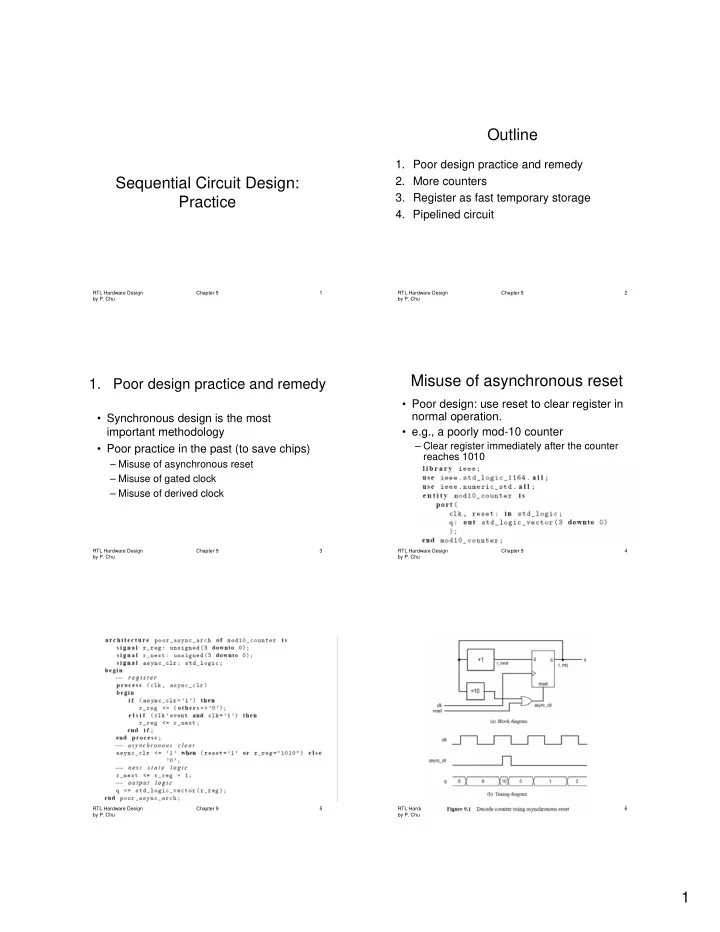
Misuse of asynchronous reset
- Poor design: use reset to clear register in
normal operation.
- e.g., a poorly mod-10 counter
– Clear register immediately after the counter reaches 1010
RTL Hardware Design by P. Chu Chapter 9 5 RTL Hardware Design by P. Chu Chapter 9 6