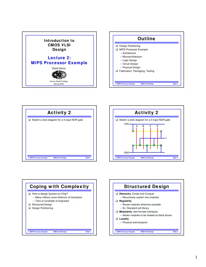
outline
play

Outline Introduction to CMOS VLSI Design Partitioning Design - PDF document

Outline Introduction to CMOS VLSI Design Partitioning Design MIPS Processor Example Architecture Microarchitecture Lecture 2: Logic Design MIPS Processor Example Circuit Design Physical Design David Harris


  1. Outline Introduction to CMOS VLSI � Design Partitioning Design � MIPS Processor Example – Architecture – Microarchitecture Lecture 2: – Logic Design MIPS Processor Example – Circuit Design – Physical Design David Harris � Fabrication, Packaging, Testing Harvey Mudd College Spring 2004 2: MIPS Processor Example CMOS VLSI Design Slide 2 Activity 2 Activity 2 � Sketch a stick diagram for a 4-input NOR gate � Sketch a stick diagram for a 4-input NOR gate VDD D A B C Y GND 2: MIPS Processor Example CMOS VLSI Design Slide 3 2: MIPS Processor Example CMOS VLSI Design Slide 4 Coping w ith Complexity Structured Design � How to design System-on-Chip? � Hierarchy : Divide and Conquer – Many millions (soon billions!) of transistors – Recursively system into modules � Regularity – Tens to hundreds of engineers � Structured Design – Reuse modules wherever possible � Design Partitioning – Ex: Standard cell library � Modularity : well-formed interfaces – Allows modules to be treated as black boxes � Locality – Physical and temporal 2: MIPS Processor Example CMOS VLSI Design Slide 5 2: MIPS Processor Example CMOS VLSI Design Slide 6 1

  2. Design Partitioning Gajski Y-Chart � Architecture : User’s perspective, what does it do? – Instruction set, registers – MIPS, x86, Alpha, PIC, ARM, … � Microarchitecture – Single cycle, multcycle, pipelined, superscalar? � Logic : how are functional blocks constructed – Ripple carry, carry lookahead, carry select adders � Circuit : how are transistors used – Complementary CMOS, pass transistors, domino � Physical : chip layout – Datapaths, memories, random logic 2: MIPS Processor Example CMOS VLSI Design Slide 7 2: MIPS Processor Example CMOS VLSI Design Slide 8 MIPS Architecture Instruction Set � Example: subset of MIPS processor architecture – Drawn from Patterson & Hennessy � MIPS is a 32-bit architecture with 32 registers – Consider 8-bit subset using 8-bit datapath – Only implement 8 registers ($0 - $7) – $0 hardwired to 00000000 – 8-bit program counter 2: MIPS Processor Example CMOS VLSI Design Slide 9 2: MIPS Processor Example CMOS VLSI Design Slide 10 Instruction Encoding Fibonacci (C) � 32-bit instruction encoding f 0 = 1; f -1 = -1 – Requires four cycles to fetch on 8-bit datapath f n = f n-1 + f n-2 f = 1, 1, 2, 3, 5, 8, 13, … format example encoding 6 5 5 5 5 6 R add $rd, $ra, $rb 0 ra rb rd 0 funct 6 5 5 16 I beq $ra, $rb, imm op ra rb imm 6 26 J j dest op dest 2: MIPS Processor Example CMOS VLSI Design Slide 11 2: MIPS Processor Example CMOS VLSI Design Slide 12 2

  3. Fibonacci (Assembly) Fibonacci (Assembly) � 1 st statement: n = 8 � How do we translate this to assembly? 2: MIPS Processor Example CMOS VLSI Design Slide 13 2: MIPS Processor Example CMOS VLSI Design Slide 14 Fibonacci (Binary) Fibonacci (Binary) � 1 st statement: addi $3, $0, 8 � Machine language program � How do we translate this to machine language? – Hint: use instruction encodings below format example encoding 6 5 5 5 5 6 add $rd, $ra, $rb 0 ra rb rd 0 funct R 6 5 5 16 I beq $ra, $rb, imm op ra rb imm 6 26 J j dest op dest 2: MIPS Processor Example CMOS VLSI Design Slide 15 2: MIPS Processor Example CMOS VLSI Design Slide 16 MIPS Microarchitecture Multicycle Controller � Multicycle µ architecture from Patterson & Hennessy Instruction fetch 0 1 2 3 MemRead MemRead MemRead MemRead Instruction decode/ register fetch ALUSrcA = 0 ALUSrcA = 0 ALUSrcA = 0 ALUSrcA = 0 IorD = 0 IorD = 0 IorD = 0 IorD = 0 4 IRWrite3 IRWrite2 IRWrite1 IRWrite0 ALUSrcB = 01 ALUSrcB = 01 ALUSrcB = 01 ALUSrcB = 01 ALUSrcA = 0 PCWriteCond PCSource ALUOp = 00 ALUOp = 00 ALUOp = 00 ALUOp = 00 ALUSrcB = 11 PCEn PCWrite PCWrite PCWrite PCWrite ALUOp = 00 PCWrite ALUOp PCSource = 00 PCSource = 00 PCSource = 00 PCSource = 00 IorD Outputs ALUSrcB MemRead (Op = 'BEQ') (Op = R-type) (Op = 'J') ALUSrcA Control Reset MemWrite RegWrite (Op = 'LB') or (Op = 'SB') MemtoReg Memory address Branch Jump Op RegDst computation IRWrite[3:0] Execution completion completion [5: 0] 0 5 9 11 12 M ALUSrcA = 1 Jump 1 u 6 8 ALUSrcA = 1 ALUSrcA =1 ALUSrcB = 00 Instruction [ 5 : 0] address x PCWrite Shift ALUSrcB = 10 ALUSrcB = 00 ALUOp = 01 2 PCSource = 10 left 2 ALUOp = 00 PCWriteCond ALUOp= 10 Instruction PCSource = 01 [31:26] PC 0 (Op = 'S B') 0 (Op = 'L B') Instruction Read M M [25 : 21] register 1 u Address u x Read x Instruction Read A 1 Memory data 1 Zero Memory Memory [20 : 16] register 2 1 ALU access access R-type completion MemData 0 Registers ALU ALUOut Instruction M Write Read result 6 8 10 B [15: 0] Instruction u register data 2 0 Write [15: 11] x RegDst = 1 Instruction Write 1 1 M MemRead MemWrite data 1 u RegWrite register data IorD = 1 IorD = 1 2 x MemtoReg = 0 0 Instruction 3 [7: 0] M u x Memory 1 Write-back step data 7 ALU register control ALUControl RegDst=0 RegWrite MemtoReg=1 Instruction [5: 0] 2: MIPS Processor Example CMOS VLSI Design Slide 17 2: MIPS Processor Example CMOS VLSI Design Slide 18 3

  4. Logic Design Block Diagram � Start at top level PCEn PCWriteCond PCWrite PCSource ALUOp MemRead IorD Outputs ALUSrcB MemWrite Control ALUSrcA MemtoReg Op RegWrite RegDst IRWrite[3:0] [5: 0] 0 Instruction [5: 0] 6 8 address Jump u x M 1 Instruction left 2 Shift 2 PC 0 [31:26] 0 u M Address [25: 21] Instruction register 1 Read M u memwrite 1 x Memory [20: 16] Instruction Read register 2 data 1 Read A x 1 Zero MemData Instruction M 0 Write Registers Read B ALU result ALU ALUOut – Hierarchically decompose MIPS into units Write Instruction [15: 0] [15: 11] Instruction x u register Write data 2 1 1 M 0 data register 1 data 2 u x Instruction [7: 0] M 0 3 Memory 1 x u memread register data ALU control ALUControl Instruction [5: 0] � Top-level interface controller aluop[1:0] alucontrol memread op[5:0] zero alusrca alusrcb[1:0] pcen pcsource[1:0] memtoreg regdst iord regwrite irwrite[3:0] funct[5:0] alucontrol[2:0] 2-phase crystal ph1 memwrite clock oscillator MIPS generator ph2 8 adr processor ph1 8 external writedata ph2 reset memory 8 memdata reset datapath adr[7:0] writedata[7:0] memdata[7:0] 2: MIPS Processor Example CMOS VLSI Design Slide 19 2: MIPS Processor Example CMOS VLSI Design Slide 20 Hierarchical Design HDLs mips � Hardware Description Languages – Widely used in logic design controller alucontrol datapath – Verilog and VHDL standard bitslice zipper � Describe hardware using code cell library – Document logic functions – Simulate logic before building alu inv4x flop ramslice – Synthesize code into gates and layout fulladder or2 and2 mux4 • Requires a library of standard cells nor2 inv nand2 mux2 tri 2: MIPS Processor Example CMOS VLSI Design Slide 21 2: MIPS Processor Example CMOS VLSI Design Slide 22 Verilog Example Circuit Design module fulladder( input a, b, c, � How should logic be implemented? a b c output s, cout); a b – NANDs and NORs vs. ANDs and ORs? sum cout c carry – Fan-in and fan-out? s sum s1(a, b, c, s); fulladder – How wide should transistors be? cout s carry c1(a, b, c, cout); � These choices affect speed, area, power endmodule � Logic synthesis makes these choices for you module carry( input a, b, c, – Good enough for many applications output cout) – Hand-crafted circuits are still better assign cout = (a&b) | (a&c) | (b&c); endmodule 2: MIPS Processor Example CMOS VLSI Design Slide 23 2: MIPS Processor Example CMOS VLSI Design Slide 24 4

Download Presentation
Download Policy: The content available on the website is offered to you 'AS IS' for your personal information and use only. It cannot be commercialized, licensed, or distributed on other websites without prior consent from the author. To download a presentation, simply click this link. If you encounter any difficulties during the download process, it's possible that the publisher has removed the file from their server.

Recommend


More recommend