
SLIDE 1
William Sandqvist william@kth.se
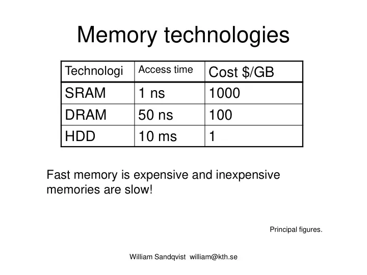
Memory technologies
Technologi
Access time
Cost $/GB SRAM 1 ns 1000 DRAM 50 ns 100 HDD 10 ms 1
Fast memory is expensive and inexpensive memories are slow!
Principal figures.
Memory technologies Access time Technologi Cost $/GB SRAM 1 ns - - PowerPoint PPT Presentation
Memory technologies Access time Technologi Cost $/GB SRAM 1 ns 1000 DRAM 50 ns 100 HDD 10 ms 1 Fast memory is expensive and inexpensive memories are slow! Principal figures. William Sandqvist william@kth.se Memory Hierarchy
William Sandqvist william@kth.se
Access time
Principal figures.
William Sandqvist william@kth.se
A three-level memory hierarchy. The faster memory types are used as "buffers" against the slower.
Principle
Primary memory Secondary memory
William Sandqvist william@kth.se
Memory: N words, widh M bits Memorychip: p words, widh q bits
p, q N, M
Words Widh Number of chips
William Sandqvist william@kth.se
Each bit in a CMOS SRAM consists of a latch circuit made up
The memory cell is basically a SR-latch.
William Sandqvist william@kth.se
Each bit in a DRAM consists of a transistor and a capacitor. A charged capacitor leaks charge after a while. Periodically, all the capacitors must be searched and those who have charge left must then be reloaded. This is called
within the memory.
William Sandqvist william@kth.se
Trench Capacitor
William Sandqvist william@kth.se
32M 25×220 = 225, 25 address bits
addressing, 13-bit RAS (row), 10 bit CAS (columns), two bank bits BA0 and BA1. Burst can be 2, 4, 8 Bytes. Chip 256Mbit (32M×8) Synchronously, using the bus clock. Double-edge triggered for double data rate ck + ck (even lower power).
William Sandqvist william@kth.se
William Sandqvist william@kth.se
Column address counter can quickly address
memory can moore quickly deliver a burst with several bytes in sequence, than an totaly random acess.
William Sandqvist william@kth.se
(2 TBUS are Waitstates)
It's important to have proper use of all fetched words - otherwise you are wasting bus clock cycles with the Burst method!
William Sandqvist william@kth.se
a) How many chips are needed for 256M×64? Chip 256Mbit (32M×8)
William Sandqvist william@kth.se
Memory N = 256M M = 64 bits. Chip p = 32M q = 8 bits. Number of columns k = M/q = 64/8 = 8. Number of rows r = N/p = 256M/32M = 8. Number of chips K = r × k = 8×8 = 64. a) How many chips are needed for 256M×64? Chip 256Mbit (32M×8)
b) How many chips are needed for 512M×72?
William Sandqvist william@kth.se
Chip 256Mbit (32M×8)
Memory N = 512M M = 72 bits. Chip p = 32M q = 8 bits. Number of columns k = M/q = 72/8 = 9. Number of rows r = N/p = 512M/32M = 16. Number of chips K = r × k = 9 ×1 6 = 144.
William Sandqvist william@kth.se
Chip 256Mbit (32M×8) b) How many chips are needed for 512M×72?
Memory N = 512M M = 72 bits. Chip p = 32M q = 8 bits. Number of columns k = M/q = 72/8 = 9. Number of rows r = N/p = 512M/32M = 16. Number of chips K = r × k = 9 ×1 6 = 144.
William Sandqvist william@kth.se
Chip 256Mbit (32M×8) b) How many chips are needed for 512M×72? The "unusual" bit width 72 (= 64 + 8). The 8 extra bits are used for correcting single faults, and to detect double faults. (In this way, even capsules small errors could be used as the error can be corrected. They would otherwise have to be discarded).
Memory N = 512M M = 72 bits. Chip p = 32M q = 8 bits. Number of columns k = M/q = 72/8 = 9. Number of rows r = N/p = 512M/32M = 16. Number of chips K = r × k = 9 ×1 6 = 144.
William Sandqvist william@kth.se
Chip 256Mbit (32M×8) b) How many chips are needed for 512M×72? The "unusual" bit width 72 (= 64 + 8). The 8 extra bits are used for correcting single faults, and to detect double faults. (In this way, even capsules small errors could be used as the error can be corrected. They would otherwise have to be discarded). Or will a expensive memory be good even if some of the memory cells "wear out" over time.
William Sandqvist william@kth.se
Decoder 3-to-8 ROM 4M 512k × 8 bit ROM: RAM: SRAM 4M 512k × 8 bit Suppose that the ROM and the SRAM is to be connected to a 16-bit microprocessor having 24 bit addressing.
Micro- processor
William Sandqvist william@kth.se
How big is the figure SRAM, and which is the address area expressed in hexadecimal numbers
Micro- processor
William Sandqvist william@kth.se
How big is the figure SRAM, and which is the address area expressed in hexadecimal numbers
Micro- processor
p = 512k q = 8 bits
r = 3 k = 2 K = 2 × 3 = 6 M = k × q = 2 × 8 = 16 bits N = p × r = 512k × 3 = 1,5M
William Sandqvist william@kth.se
How big is the figure SRAM, and which is the address area expressed in hexadecimal numbers
Micro- processor
p = 512k q = 8 bits
r = 3 k = 2 K = 2 × 3 = 6 M = k × q = 2 × 8 = 16 bits N = p × r = 512k × 3 = 1,5M
William Sandqvist william@kth.se
Micro- processor
William Sandqvist william@kth.se
Micro- processor
William Sandqvist william@kth.se
Micro- processor
SRAM adress range: A80000 - BFFFFF
Change the address range to 980000 – AFFFFF ? 980000 1001|1000|0000|0000|0000|0000| AFFFFF 1010|1111|1111|1111|1111|1111|
William Sandqvist william@kth.se
Change the address range to 980000 – AFFFFF ? 980000 1001|1000|0000|0000|0000|0000| AFFFFF 1010|1111|1111|1111|1111|1111|
William Sandqvist william@kth.se
Change the address range to 980000 – AFFFFF ? 980000 1001|1000|0000|0000|0000|0000| AFFFFF 1010|1111|1111|1111|1111|1111|
William Sandqvist william@kth.se
”10|011” → ”3” ”10|101” → ”5”
Change the address range to 980000 – AFFFFF ? 980000 1001|1000|0000|0000|0000|0000| AFFFFF 1010|1111|1111|1111|1111|1111|
William Sandqvist william@kth.se
”10|011” → ”3” ”10|101” → ”5”
Micro- processor
Change the address range to 480000 – 5FFFFF ?
William Sandqvist william@kth.se
Change the address range to 480000 – 5FFFFF ?
William Sandqvist william@kth.se
480000 0100|1000|0000|0000|0000|0000| 5FFFFF 0101|1111|1111|1111|1111|1111|
Change the address range to 480000 – 5FFFFF ?
William Sandqvist william@kth.se
480000 0100|1000|0000|0000|0000|0000| 5FFFFF 0101|1111|1111|1111|1111|1111| ”01|001” → ”1” ”01|011” → ”3”
Change the address range to 480000 – 5FFFFF ?
William Sandqvist william@kth.se
480000 0100|1000|0000|0000|0000|0000| 5FFFFF 0101|1111|1111|1111|1111|1111| ”01|001” → ”1” ”01|011” → ”3”
Micro- processor
Change the address range to 480000 – 5FFFFF ?
William Sandqvist william@kth.se
480000 0100|1000|0000|0000|0000|0000| 5FFFFF 0101|1111|1111|1111|1111|1111| ”01|001” → ”1” ”01|011” → ”3”
Micro- processor
William Sandqvist william@kth.se
Most often a processor reads its first instruction from address 0, then there must be a ROM at that address. Suppose a ROM 2M × 16 bitar address range 000000 … and forward. ROM Chip 512k×8.
numbers.
William Sandqvist william@kth.se
Most often a processor reads its first instruction from address 0, then there must be a ROM at that address. Suppose a ROM 2M × 16 bitar address range 000000 … and forward. ROM Chip 512k×8.
numbers. Memory: N = 2 M (4⋅512k) word is M = 16 bitar Memory chip: p = 512 k word is q = 8 bitar
William Sandqvist william@kth.se
Micro- processor
William Sandqvist william@kth.se
Micro- processor
William Sandqvist william@kth.se
Micro- processor
William Sandqvist william@kth.se
Micro- processor
William Sandqvist william@kth.se
William Sandqvist william@kth.se
00ab|cmmm|mmmm|mmmm|mmmm|mmmm 0000|0000|0|0|0|0 - 0000|0111|F|F|F|F 000000-07FFFF 0000|1000|0|0|0|0 - 0000|1111|F|F|F|F 080000-0FFFFF 0001|0000|0|0|0|0 - 0001|0111|F|F|F|F 100000-17FFFF 0001|1000|0|0|0|0 - 0001|1111|F|F|F|F 180000-1FFFFF
William Sandqvist william@kth.se
00ab|cmmm|mmmm|mmmm|mmmm|mmmm 0000|0000|0|0|0|0 - 0000|0111|F|F|F|F 000000-07FFFF 0000|1000|0|0|0|0 - 0000|1111|F|F|F|F 080000-0FFFFF 0001|0000|0|0|0|0 - 0001|0111|F|F|F|F 100000-17FFFF 0001|1000|0|0|0|0 - 0001|1111|F|F|F|F 180000-1FFFFF Totaly ROM 000000 – 1FFFFF
William Sandqvist william@kth.se
00ab|cmmm|mmmm|mmmm|mmmm|mmmm 0010|0000|0|0|0|0 - 0010|0111|F|F|F|F 200000-27FFFF 0010|1000|0|0|0|0 - 0010|1111|F|F|F|F 280000-2FFFFF 0011|0000|0|0|0|0 - 0011|0111|F|F|F|F 300000-37FFFF 0011|1000|0|0|0|0 - 0011|1111|F|F|F|F 380000-3FFFFF
William Sandqvist william@kth.se
00ab|cmmm|mmmm|mmmm|mmmm|mmmm 0010|0000|0|0|0|0 - 0010|0111|F|F|F|F 200000-27FFFF 0010|1000|0|0|0|0 - 0010|1111|F|F|F|F 280000-2FFFFF 0011|0000|0|0|0|0 - 0011|0111|F|F|F|F 300000-37FFFF 0011|1000|0|0|0|0 - 0011|1111|F|F|F|F 380000-3FFFFF I/O
William Sandqvist william@kth.se
00ab|cmmm|mmmm|mmmm|mmmm|mmmm 0010|0000|0|0|0|0 - 0010|0111|F|F|F|F 200000-27FFFF 0010|1000|0|0|0|0 - 0010|1111|F|F|F|F 280000-2FFFFF 0011|0000|0|0|0|0 - 0011|0111|F|F|F|F 300000-37FFFF 0011|1000|0|0|0|0 - 0011|1111|F|F|F|F 380000-3FFFFF
I/O
William Sandqvist william@kth.se
00ab|cmmm|mmmm|mmmm|mmmm|mmmm 0010|0000|0|0|0|0 - 0010|0111|F|F|F|F 200000-27FFFF 0010|1000|0|0|0|0 - 0010|1111|F|F|F|F 280000-2FFFFF 0011|0000|0|0|0|0 - 0011|0111|F|F|F|F 300000-37FFFF 0011|1000|0|0|0|0 - 0011|1111|F|F|F|F 380000-3FFFFF Possible SRAM+I/O adresser 200000 – 3FFFFF
I/O
Peripheral circuit connected as a small RAM. Only the 8 least significant bits
William Sandqvist william@kth.se
Peripherals, I/O, are often connected to a CPU as if they were memory chips (though with only a few "memory cells").
from the 8 built-in registers.
William Sandqvist william@kth.se
I/O adresses, at the decoder output ”4”, 200000 – 27FFFF according to the earlier task.
Micro- processor
3 4 5 6 7 8 9 10 11 12 13 14 15 16 17 18
A A A A A A A A A A A A A A A A ⋅ ⋅ ⋅ ⋅ ⋅ ⋅ ⋅ ⋅ ⋅ ⋅ ⋅ ⋅ ⋅ ⋅ ⋅ RS2RS1RS0
William Sandqvist william@kth.se
Decoder output ”4” Remains to decode:
William Sandqvist william@kth.se
Micro- processor
William Sandqvist william@kth.se
Micro- processor
A bit too many inputs?
William Sandqvist william@kth.se
Addressing becomes ambiguous!
William Sandqvist william@kth.se
Addressing becomes ambiguous!
For full decoding, we used a &-gate with 17 inputs! Sometimes you make a partial
inputs. I/O device addressing is ambiguous, it can be addressed with many different addresses, but the one who writes the program code determines which addresses to use. The main thing is to ensure that the I/O device addresses do not collide with any other device addresses.
William Sandqvist william@kth.se
William Sandqvist william@kth.se
Since the I/O devices are not true memories - it can seem as if the content can be changed "by itself" - so when you write computer programs you need to "help" the compiler to understand this. It could be done by declaring these adresses as volatile. This, you will meet in Computer Engineering course.
William Sandqvist william@kth.se
= ) 27 , 26 , 25 , 24 , 18 , 16 , 15 , 14 , 13 , 12 , 11 , 9 ( ) , , , , (
1 2 3 4
m x x x x x f
William Sandqvist william@kth.se
= ) 27 , 26 , 25 , 24 , 18 , 16 , 15 , 14 , 13 , 12 , 11 , 9 ( ) , , , , (
1 2 3 4
m x x x x x f ? ? ) , , , , (
1 2 3 4
= = f f x x x x x f ? ) , , , , (
1 2 3 4
= f x x x x x f
William Sandqvist william@kth.se
= ) 27 , 26 , 25 , 24 , 18 , 16 , 15 , 14 , 13 , 12 , 11 , 9 ( ) , , , , (
1 2 3 4
m x x x x x f ? ? ) , , , , (
1 2 3 4
= = f f x x x x x f ? ) , , , , (
1 2 3 4
= f x x x x x f
William Sandqvist william@kth.se
= ) 27 , 26 , 25 , 24 , 18 , 16 , 15 , 14 , 13 , 12 , 11 , 9 ( ) , , , , (
1 2 3 4
m x x x x x f ? ? ) , , , , (
1 2 3 4
= = f f x x x x x f ? ) , , , , (
1 2 3 4
= f x x x x x f
2 4 2 3 2 3 4
x x x x x x x x x f + + =
William Sandqvist william@kth.se
= ) 27 , 26 , 25 , 24 , 18 , 16 , 15 , 14 , 13 , 12 , 11 , 9 ( ) , , , , (
1 2 3 4
m x x x x x f ? ? ) , , , , (
1 2 3 4
= = f f x x x x x f ? ) , , , , (
1 2 3 4
= f x x x x x f
William Sandqvist william@kth.se
= ) 27 , 26 , 25 , 24 , 18 , 16 , 15 , 14 , 13 , 12 , 11 , 9 ( ) , , , , (
1 2 3 4
m x x x x x f ? ? ) , , , , (
1 2 3 4
= = f f x x x x x f ? ) , , , , (
1 2 3 4
= f x x x x x f
William Sandqvist william@kth.se
= ) 27 , 26 , 25 , 24 , 18 , 16 , 15 , 14 , 13 , 12 , 11 , 9 ( ) , , , , (
1 2 3 4
m x x x x x f ? ? ) , , , , (
1 2 3 4
= = f f x x x x x f ? ) , , , , (
1 2 3 4
= f x x x x x f
2 4 2 4 3 3 4
x x x x x x x x x f + + + =
William Sandqvist william@kth.se
Bring out the Boolean equations for a network at minimal SP-form which transforms a three-bit binary coded number X (x2, x1, x0) to a binary coded six bit number U (u5, u4, u3, u2, u1, u0) which is equal to the square of the number U = X 2.
William Sandqvist william@kth.se
William Sandqvist william@kth.se
Of truth table it shows that u1 always is equal to 0. u1 uotput could therefore be connected to 0V (ground) so it will get the constant 0. One can further see that u0 always is the same as x0. u0 output can therfore be connected directly to x0 input.
William Sandqvist william@kth.se
A stepper motor is a digital component that is driven by pulses. Stepper motors are usually connected to a counter counting Gray code. Figure calculator also has a mode-input, m1m0. m1m0 = 00 → Reset (fixed position) m1m0 = 01 → count up (cw) m1m0 = 10 → count down (ccw) m1m0 = 11 → Preset (another fixed position)
William Sandqvist william@kth.se
Sometimes you write boolean conditions instead of just the numbers at the arrows. In the figure, both the condition and numbers are used. m1m0 = 00 → Reset (fixed position) m1m0 = 01 → count up (cw) m1m0 = 10 → count down (ccw) m1m0 = 11 → Preset (another fixed position)
William Sandqvist william@kth.se
William Sandqvist william@kth.se
One aproach for implementing integer division is to perform repeated subtraction as indicated in pseudo-code. Q = 0; R = A While ((R – B) ≥ 0) do R = R – B; Q = Q + 1; End while; a) Give an ASM chart that represents the pseudo-code. b) Show the datapath circuit corresponding to part (a). c) Give the ASM chart for the control circuit corresponding to part (b).
ASM method consists of the following steps:
desired circuit function.
William Sandqvist william@kth.se
Figure 8.86. Elements used in ASM charts.
Output signals
(Moore type) State name Condition expression 0 (False) 1 (True) Conditional outputs
(a) State box (b) Decision box (c) Conditional output box
William Sandqvist william@kth.se
William Sandqvist william@kth.se
Q = 0; R = A While ((R – B) ≥ 0) do R = R – B; Q = Q + 1; End while;
William Sandqvist william@kth.se
Q = 0; R = A While ((R – B) ≥ 0) do R = R – B; Q = Q + 1; End while;
RESET
Q←0 Start? Load R←A Load B
S1
1
William Sandqvist william@kth.se
Q = 0; R = A While ((R – B) ≥ 0) do R = R – B; Q = Q + 1; End while;
Wait for start! RESET
Q←0 Start? Load R←A Load B
S1
1
William Sandqvist william@kth.se
Q = 0; R = A While ((R – B) ≥ 0) do R = R – B; Q = Q + 1; End while;
Wait for start! RESET
Q←0 Start? Load R←A Load B
S1
1
? ≥ − B R
S2
1 R←R-B Q←Q+1
William Sandqvist william@kth.se
Q = 0; R = A While ((R – B) ≥ 0) do R = R – B; Q = Q + 1; End while;
Wait for start! RESET
Q←0 Start? Load R←A Load B
S1
1
? ≥ − B R
S2
1 R←R-B Q←Q+1
Subtract!
William Sandqvist william@kth.se
Q = 0; R = A While ((R – B) ≥ 0) do R = R – B; Q = Q + 1; End while;
Wait for start! RESET
Q←0 Start? Load R←A Load B
S1
1
? ≥ − B R
S2
1 R←R-B Q←Q+1
Subtract! Done?
William Sandqvist william@kth.se
Q = 0; R = A While ((R – B) ≥ 0) do R = R – B; Q = Q + 1; End while;
RESET
Q←0 Start? Load R←A Load B
S1
1
? ≥ − B R
S2
1 R←R-B Q←Q+1
William Sandqvist william@kth.se
Q = 0; R = A While ((R – B) ≥ 0) do R = R – B; Q = Q + 1; End while;
RESET
Q←0 Start? Load R←A Load B
S1
1
? ≥ − B R
S2
1 R←R-B Q←Q+1
Klar
Start?
S3
1
William Sandqvist william@kth.se
Q = 0; R = A While ((R – B) ≥ 0) do R = R – B; Q = Q + 1; End while;
RESET
Q←0 Start? Load R←A Load B
S1
1
? ≥ − B R
S2
1 R←R-B Q←Q+1
Wait for Start to be released, to restart.
Done
Start?
S3
1
William Sandqvist william@kth.se
) (
1 2 3 3 3 4
s s s s Z s N c c V Y X + + + = = ⊕ = − V N Y X V N Z V N Z Y X V N Z Y X V N Y X Z Y X ⊕ ⇒ ≥ ⊕ ⋅ = ⊕ + ⇒ > ⊕ + ⇒ ≤ ⊕ ⇒ < = ⇒ = ) ( 1
This is how a computer can do the most common comparisons …
William Sandqvist william@kth.se
Q = 0; R = A While ((R – B) ≥ 0) do R = R – B; Q = Q + 1; End while;
William Sandqvist william@kth.se
RESET
LoadQ LoadB RBdiff_sel=0 LoadR_A
Start?
S1
1
S2
1 LoadR_A
Done
Start?
S3
1
RBdiff_sel=1 R_GE_B
William Sandqvist william@kth.se