Medical devices vs 6 Cardinal Health 12.4 6 Broadcom 15.5 6 - - PDF document

medical devices vs
SMART_READER_LITE
LIVE PREVIEW

Medical devices vs 6 Cardinal Health 12.4 6 Broadcom 15.5 6 - - PDF document

2019/2/26 Context Challenges in the Design of Integrated Circuits for Wireless Power Delivery Medical devices vs Semiconductors industries and Information Transfer in How to develop a medical instrument, equipment, or device Implantable


slide-1
SLIDE 1

2019/2/26 1

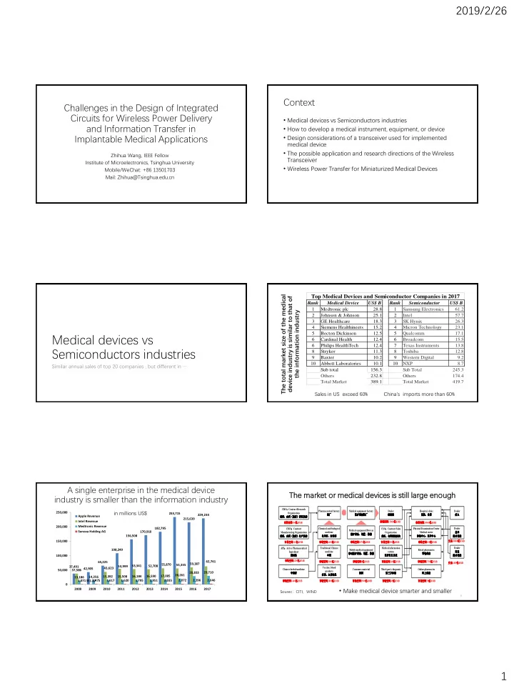
Challenges in the Design of Integrated Circuits for Wireless Power Delivery and Information Transfer in Implantable Medical Applications

Zhihua Wang, IEEE Fellow Institute of Microelectronics, Tsinghua University Mobile/WeChat: +86 13501703 Mail: Zhihua@Tsinghua.edu.cn

Context

  • Medical devices vs Semiconductors industries
  • How to develop a medical instrument, equipment, or device
  • Design considerations of a transceiver used for implemented

medical device

  • The possible application and research directions of the Wireless

Transceiver

  • Wireless Power Transfer for Miniaturized Medical Devices

Medical devices vs Semiconductors industries

Similar annual sales of top 20 companies , but different in …

The total market size of the medical device industry is similar to that of the information industry

Rank Medical Device US$ B Rank Semiconductor US$ B 1 Medtronic plc 28.8 1 Samsung Electronics 61.2 2 Johnson & Johnson 25.1 2 Intel 57.7 3 GE Healthcare 18.3 3 SK Hynix 26.3 4 Siemens Healthineers 15.2 4 Micron Technology 23.1 5 Becton Dickinson 12.5 5 Qualcomm 17.1 6 Cardinal Health 12.4 6 Broadcom 15.5 6 Philips HealthTech 12.4 7 Texas Instruments 13.8 8 Stryker 11.3 8 Toshiba 12.8 9 Baxter 10.2 9 Western Digital 9.2 10 Abbott Laboratories 10.1 10 NXP 8.7 Sub total 156.3 Sub Total 245.3 Others 232.8 Others 174.4 Total Market 389.1 Total Market 419.7

Top Medical Devices and Semiconductor Companies in 2017 Sales in US exceed 60% China’s imports more than 60%

37,491 42,905 65,225 108,249 156,508 170,910 182,795 233,715 215,639 229,234 37,586 351.27 43,623 53,999 53,341 52,708 55,870 55,355 59,387 62,761 13,186 14,256 15,392 15,508 16,184 16,590 17,005 20,261 28,833 29,710 1,071 1,475 1,617 1,620 1,795 1,951 2,035 2,072 2,396 2,646 50,000 100,000 150,000 200,000 250,000 2008 2009 2010 2011 2012 2013 2014 2015 2016 2017 Apple Revenue Intel Revenue Medtronic Revenue Sonova Holding AG

A single enterprise in the medical device industry is smaller than the information industry

in millions US$

The market et or medic ical al devic ices es is still l large e enoug ugh

CRO:Contract Research Organization 委托、合同(临床)研究机构 CMO:Contract Manufacturing Organization 委托、合同(临床)生产机构 CSO:Contract Sales Organization 委托、合同销售机构 API:Active Pharmaceutical Ingredient 原料药 Chinese herbal medicine 中药材 Pharmaceutical factory 药厂 Chemical and biological medicine 化学药、生物药 Traditional Chinese medicine 中药 Vaccine, blood products 疫苗、血液制品 Medical equipment factory 医疗器械药厂 Medical equipment/Devices 医疗设备、装置、器械 Mobile medical equipment 移动医疗设备、装置、器械 Consumes material 耗材 Dealer 经销商 Medical information system 医疗信息系统 Third party diagnosis 第三方诊断 Hospital, clinic 医院、诊所 Physical Examination Center Medical center 体检中心、医学中心 Retail pharmacies 零售药店 Online pharmacies 网上药店 Dealer 病人 Dealer 基本 医疗保险 Dealer 商业 医疗保险 支出1400亿RMB 支出10000亿RMB 市场空间29000亿RMB 市场空间150亿RMB 市场空间2750亿RMB 市场空间70亿RMB 市场空间15000亿RMB 市场空间150亿RMB 市场空间240亿RMB 市场空间45亿RMB 市场空间2070亿RMB 市场空间8亿RMB 市场空间1500亿RMB 市场空间2800亿RMB 市场空间5800亿RMB 市场空间6450亿RMB 市场空间530亿RMB 市场空间110亿RMB 市场空间4200亿RMB 市场空间1460亿RMB

Sourec:CITI,WIND

6

  • Make medical device smarter and smaller
slide-2
SLIDE 2

2019/2/26 2 How to develop a medical instrument, equipment, or device

With the Integrated Circuit is Enabling Technology

7

What is a medical device

  • An instrument, apparatus, implement, machine,

contrivance, implanted in vitro reagent, or other similar or related article, including a component part, or accessory which is:

  • Recognized in the official National Formulary
  • Intended for use in the diagnosis of disease or other

conditions

  • Intended to affect the structure or any function of the

body of man or other animals

8

Classification of medical Devices

  • Class I: General controls
  • Class II: General controls with special controls
  • infusion pumps, and surgical drapes…
  • Class III: General controls and premarket approval
  • implantable pacemaker, pulse generators, automated

external defibrillators…

9

Research and Development of an medical system

Specification Design Prototype/ Product Verification Small Production Technology Transfer Design Review Validation Large Production Research Idea / Concept

10

A Medical System with Portable and/or Implantable Medical Devices

Deep Brain Neurostimulator Cochlear implant Endoscopic Capsule Others IMDs Gastric stimulator

Portable and/or Implantable Medical Devices - IMDs

Controller / Programmer Display / control unit

External Host Devices - EHDs

(Terms and Definitions)

11

Composition or Development Platform

  • Communication protocols and modules
  • information security
  • Sensing modules
  • Pacing modules
  • Wireless battery recharge module
  • Lead impedance measurement modules
  • Accelerometer modules
  • FW download module
  • RTC module

12

slide-3
SLIDE 3

2019/2/26 3

A Portable and/or Implantable Device

  • Electronic implantable medical devices (IMD) are

designed to be fully or partially implanted in the human bodies through surgeries[1], and remain in bodies for several hours to several years or even permanently after the surgical intervention.

[1] R. Ritter, J. Handwerker, T. Liu, and M. Ortmanns, “Telemetry for Implantable Medical Devices,” IEEE SOLID-STATE CIRCUITS MAGAZINE, vol. 6, Issue. 2, pp. 47-51, Spring 2014.

What is a Portable and/or Implantable Medical Device?

13

Examples of Portable and/or Implantable Medical Devices

Total hip replacement capsule endoscopy Robot hand Cochlear implants Nerve Stimulator Total Knee replacement

14

About the information security - Mostly at the system level and implemented in software

Confidentiality Integrity Availability Accountability CIAA policy

15

Enabling Technology is Integrated Circuit

  • Information Sciences:

Acquisition processing, Storage Transmission

  • f (medical and life )

signals Analog Front End ADC DSP Radio μC Sensor Power management, battery, harvester

16

Design considerations of a transceiver used for implemented medical device

17

Well known implemented medical devices in clinical application

  • cardiac pacemakers,
  • implantable defibrillators,
  • Cochlear implants,
  • nerve stimulators (Functional Electrical Stimulation-FES),
  • limb function stimulation,
  • bladder stimulators,
  • Sphincter stimulators,
  • diaphragm stimulators,
  • implantable infusion pumps,
  • bio-monitoring devices such as the capsule endoscope.

18

slide-4
SLIDE 4

2019/2/26 4

Two option ions to power er an implem lemen ented ed medic ical al devic ices es

  • miniature battery, and wireless power.
  • lowering the circuit power consumption,
  • to evaluate the available space for power supply components inside IMDs,
  • The lifetime and reliability requirement, before choosing the

power type.

  • For example, a cardiac pacemaker relying on a reliable energy source

may choose a battery, while an intraocular IMD usually choose wireless power since there is no room for a battery. The requirements on the wireless transceivers for different IMDS are quite diverse, in terms of data rate, signal transmission distance, and communication directions (single direction or two-way). The data integrity and bit-error rate (BER) tolerance are also of great importance, and the poor performances on these aspects may lead to harmful and even fetal malfunction.

19

implemented medical devices power and wireless data requirements

IMDs Power consumption Target data rate Life-Time Energy Source Biomonitoring System <100 μW < 10 kb/s a few days Primary Battery Capsule endoscope <15mW >1 Mb/s 10 Hours Primary Battery Pacemaker <100 μW 10 Years Primary Battery Cardioverter-Defibrilator Cont: <100 μW; Peak: 5–10 W 10 Years Primary Battery Cochlear Processor 200 μW >100Kb/s 1 Week Rechargeable Battery Hearing Aid 100–2,000 μW 200 kb/s 1 Week Rechargeable Battery Retinal Implant 40–250 mW > 500kb/s NA Inductive Power Neural Recorder/Stimulator 1–100 mW <1 Mb/s NA Inductive Power Artificial Heart 10–100 W NA Inductive Power

20

Frequ quenc ency band d sele lection ction for implemente plemented d medica ical l device ices transc nscei eiver er desi sign gn

  • considering the huge variation of EM signal propagation characteristics through human tissues

with different frequencies. Based on FCC frequency regulations, the MedRadio band (composed of several inconsecutive bands in 401–457 MHz) has superior propagation characteristics for implants, quiet channel properties, and worldwide availability, which are the primary reasons for its popularity for implant applications. The 2.45GHz ISM band, with the mature circuit technologies, wide support for connecting to smart phones and other mobile devices, convenient access to the network, is also widely used for implantable medical systems.

Global Frequency bands Category Comments 9 – 315 kHz EU medical implant Not so allocated outside EU 13.56 MHz ISM and SRD RFID transponders for patient ID 27.12 MHz ISM and R/C Congested 40.68 MHz ISM and SRD Protocol restrictions in USA 402 – 405 MHz Medical Implant Comm. Reserved for implants 2.45 GHz ISM and SRD and microwave oven 802.11b/g (BT, Wi-Fi) 5.8 GHz ISM 802.11a Table 2. Radio standards – Implantable Medical devices

21

IMD anten enna a desi esign for IMDs

  • IMD antenna design is also very challenging due to the size and

shape restrictions, and the complicated working environment in human bodies. Since the electrical properties of the human tissues varies a lot with the patients' weight, age, posture changes, etc., the IMD antennas may adopt different sizes and shapes depending on the implantation location, which further limits the freedom of the designer

22

Implem emente ted Transc scei eivers ers for r IMD

  • 400 MHz RF transceiver
  • 2.4 GHz RF transceiver
  • Reconfigurable Sliding-Intermediate-Frequency (IF) Transceiver

for 400 MHz/2.4 GHz IEEE 802.15.6/ZigBee

  • 400 MHz/2.4 GHz TRX for dual-band communication

23

Asymm mmetr trical al RF Tran ansc sceiver er in 400M 0MHz Band

  • The data transmission from IMD to EHD sometimes requires very

high burst data rate, while the control/command information receiving requires much lower data rate

  • Asymmetrical wireless transceiver for IMD
  • High speed transmitter, very careful low power design
  • Low speed receiver
  • TX: 3Mbps MSK modulation
  • High data rate  low duty cycle for battery
  • MSK chosen for bandwidth, performance & circuit complex.
  • RX: 64kbps OOK demodulation
  • Low circuit complexity

24

slide-5
SLIDE 5

2019/2/26 5

A 400M 0MHz IMD Transc scei eiver er

25

Low Power r Transm smitt tter er with th Curren rrent t Shari ring

  • Zero-IF MSK modulator
  • DC current sharing

between IF DAC and mixer

  • Traditionally mixer and IF

DAC are cascaded

  • No traditional power

amplifier

  • Mixer directly loaded by

antenna

26

Freq equen ency Synth thesi esizer r w/ / Curren rrent t Reuse se

  • 800M LC VCO w/ self

calibration on tuning range

  • Double as the carrier

frequency to generate quadrature carriers

  • Current Reuse between

VCO & Quadrature frequency divider [1]

  • Current budget: VCO

0.6mA, all other blocks 0.2mA

27 [1] Park, et. al., “Current reusing VCO and divide-by-two frequency divider for quadrature LO generation,” IEEE Microwave & Wireless Comp. Let., Jun. 2008

Antenna Design for IMD Transceiver

  • Difficult to achieve good antenna

matching for implantable SID with traditional antenna

  • Surrounding environment affects the antenna

characteristic a lot

  • Difficult to characterize antenna’s surrounding

environment

  • In this design, an inductor serves as

antenna

  • Ctune is calibrated so that the RF port achieves

resonance

  • no traditional antenna, therefore no traditional

antenna matching

  • A virtual transformer works as

antenna

  • Inductor Lemit serves as the primary coil

emit

  • Human body serves as the secondary coil
  • The transformer has very low coupling
  • The transmitter sees very steady load, good

for circuit design (positive)

  • The transmitting loss is high (negative)
  • Our experience: if inductor Lemit has an RF ac

current of 10mA (peak to peak), PBS receiving antenna can receive >-75dBm RF signal from

  • utside body

28

Switch h betwee een n RX & TX

Qp Qn Ip In NTX_RX Wp Wn NTX_RX MIXER_RX ~50nH MIXER_TX

  • RF I/O port is calibrated for

resonance at TX mode

  • A RF peak detector is used to set

the tuning capacitor such that to have highest RF output at the RF I/O port

  • At RX mode, the load (inductor)

will see different capacitance from TX mode

  • Transistors’ working regions change

a lot  parasitic capacitance changes a lot

  • The dummy circuits in the center
  • f this figure is toggled to

compensate for the capacitance difference

  • The dummy circuit is a duplicate of

the transistors connected to RF I/O port

29

Media Access Controller

Whitening RS Encoder CRC Generation SRAM Interface Correlator and 4B5B Decode RS Decoder CRC Decoder RX FIFO TX Control RX Control TXD RXD

Media Access Controller (MAC)

SRAM MCU Transmit Processing Receive Processing Dewhitening Clock Recovery 30

slide-6
SLIDE 6

2019/2/26 6

400 MHz Transceiver for IMD’s

31

Parameters This work Supply voltage 2.5V~3.3V External Components # 7 Frequency Band 400-432 MHz Number of Channels 8 TX Bit Rate 3Mbps Power Consumption 3.9mW Power Efficiency 1.3nJ/bit RX Bit Rate 64kbps Power Consumption 12mW

  • 400 MHz wireless transmitter in 0.18

μm CMOS process

Low duty cycle ratio Reduced average power consumption (average 27 μA) 3 Mbps MSK modulation Carrier frequency 416 MHz Peak current 2.7 mA Turned on for 14 ms every second Sampling rate = 1 sps

32

  • H. Jiang et al., “A SoC with 3.9 mW 3 Mbps UHF transmitter and 240 μW MCU for capsule endoscope with bidirectional

communication,” in Proc. IEEE Asian Solid-State Circuits Conf., Beijing, China, 2010, pp. 1–4.

  • H. Jiang et al., “Implantable Wireless Intracranial Pressure Monitoring Based on Air Pressure Sensing”, Trans. Bio. Circuit and

System, 2018

  • P. Bradley, “RF Integrated Circuits for Medical Implants: Meeting the Challenge of Ultra Low-Power,” available online:

http://www.cmoset.com/uploads/Peter_Bradley.pdf

400 MHz Transceiver for IMD’s 2.4 GHz IMD Transceiver

33

  • Y. Guo et al., “A 120 pJ/bit ΔΣ-Based 2.4-GHz Transmitter Using FIR-Embedded Digital Power Amplifier, ”

IEEE Trans. Circuit and System-II., 2018

Realization of the FIR filtering using Digital Power Amp. and shift register

34

Implementation of PA network

35

  • An embedded 16-order FIR filter(for OOB noise attenuated by at least 20 dB)
  • 16 digitally controlled class-AB PA cells with each I/Q path
  • The cascode transistors as the switches of the PA cells to avoid voltage breakdown issue.
  • Each PA cell: two pseudo-differential amplifiers controlled by two internal signals EN1 and EN2

2.4 GHz Transceiver for IMD’s

36

Parameters This work ISSCC 2012 12 JSS JSSC 2017 17 TCAS AS-I 2017 17 CMOS Process 180 nm 90 nm 28 nm 90 nm Supply voltage/V 1.2 1.2 0.5/1 1 Modulation 64-QAM HS-OQPSK GFSK OOK Carrier Frequency/GHz 2.4 2.4 2.4 2.4 Data Rate/Mbps 20 2 1 1 EVM/% 11 2.3

  • 5.5

Power Consumption/mW 2.37 5.4 3.7 2.17 Power Efficiency 120 pJ/bit 1.10 nJ/bit 1.14 nJ/bit 2.17 nJ/bit TX Pout/dBm

  • 15
  • 1

0/-10

  • Y. Liu, X. Huang, M. Vidojkovic, et al., “A 2.7nJ/b multi-standard 2.3/2.4GHz polar transmitter for wireless sensor networks,” IEEE

International Solid-State Circuits Conference, Feb 2012, pp. 448-450.

  • F. W. Kuo et al., "A Bluetooth Low-Energy Transceiver With 3.7-mW All-Digital Transmitter, 2.75-mW High-IF Discrete-Time

Receiver, and TX/RX Switchable On-Chip Matching Network," in IEEE Journal of Solid-State Circuits, vol. 52, no. 4, pp. 1144- 1162, April 2017.

  • S. J. Kim; C. S. Park; S. G. Lee, "A 2.4-GHz Ternary Sequence Spread Spectrum OOK Transceiver for Reliable and Ultra-Low

Power Sensor Network Applications," in IEEE Transactions on Circuits and Systems I: Regular Papers , vol.PP, no.99, pp.1-12

slide-7
SLIDE 7

2019/2/26 7

Reconfigurable Sliding-IF Transceiver for 400 MHz/2.4 GHz IEEE 802.15.6/ZigBee for IMDs

37

  • L. Zhang, et al., “A Reconfigurable Sliding-IF Transceiver for 400 MHz/2.4 GHz IEEE 802.15.6/ZigBee WBAN Hubs With

Only 21% Tuning Range VCO,” J. Solid State Circuit, vol. 48(11), 2013, pp. 2705-2716

Wideband RF Front-end and off-chip matching circuits

  • Active shunt feedback LNA with multiple

gm enhancement

  • M1/2 provides gm
  • M3/4 enhances gm
  • M5/6 feedback for wideband matching
  • M7/8 widen resistance
  • Class AB/B/C reconfigurable PA
  • Conduction angle adjustable
  • DBPSK/DQPSK-class AB
  • OQPSK/MSK-class B/C
  • Matching circuits shared by TX/RX
  • An off-chip 1:2.5 balun needed
  • Reasonable input impedance <350 Ω to

flatten the input reflection

  • Optimum load 320 Ω
  • External 2nd order LC filter suppressing 1.4-1.5

GHz

38

Reconfigurable RX Mixer

RX HF amp-mix: Gilbert mixer

  • High frequency LO input (an amplifier while DC LO input)
  • Pseudo-differential cascode amplifier mode:
  • M14/15 off, and M13/16 biased, M11/12 common-source input

stage

  • Mixer mode
  • M13-16: active switches driven by LO.
  • LNA’s resistor load switched to a LC tank
  • filter out in-band interference
  • suppress the IM

One path of the RX LF quadrature mixer

  • PMOS input and switch transistors: good flick noise performance
  • NMOS active load: high output voltage swing
  • Common mode (CM) feedback
  • collect the redundant current
  • stabilize the output CM voltage.

39

Automatic gain control (AGC) method

AGC flow

  • 1. Set maximum RF gain
  • 2. Turn VA1 to 30~60mV
  • 3. Pre-determine IF gain
  • 4. Adjust IF gain by N dB

according to interference magnitude of VA2

  • 5. Check ADC output and

adjust VA3 to 200~600mV

40

  • J. Dong, et al. “A Fast AGC Method for Multimode Zero-IF/Sliding-IF WPAN/BAN Receivers,” IEEE

International Symposium on Circuits and Systems, 2015, pp. 1310 - 1313.

TX up-converter with PPF IQ/LO generator

  • A second order PPF
  • generate the IQ Local Osc. signals for

the HF mixer.

  • The Poly Phase Filter order and RC

values

  • trade-off: image rejection ratio VS LO

driver power consumption

  • An inductor resonate S with the PPF

equivalent capacitor

  • deliver large amplitude IQ LO signals to

the HF mixer.

  • LC tank
  • load filter out 1.4~1.5 GHz IM signal

41

Reconfigurable Sliding-IF Transceiver IMDs

42

2012 ASSCC 2013 JSSC

  • L. Zhang et al., “A low-power reconfigurable multi-band

sliding-IF transceiver for WBAN hubs in 0.18 μm CMOS,” in 2010 IEEE Asian Solid State Circuits Conf., A-SSCC, 2012, pp. 77–80.

slide-8
SLIDE 8

2019/2/26 8

400 MHz/2.4 GHz TRX for dual-band communication

43

  • Z. Weng et al., “400-MHz/2.4-GHz Combo WPAN

Transceiver IC for Simultaneous Dual-Band CommunicationWith One Single Antenna, ” IEEE Trans. Circuit and System-I, vol. 65(2), 2018, pp. 745-757

✔overcome in-band crosstalk interference

Signal al level els s and Harm rmonic Suppress ression

44

Interference Cancellation

45

2.4 GHz z band RX RF fronte ntend nd and ana nalo log baseband nd circuit cuit desig ign

46

RF frontend

  • Single-ended cascode LNA
  • Gilbert cell based mixer
  • Passive quadrature mixer

1st mixer

  • LO signal frequency: 4/5 of the

desired carrier frequency

I/Q branches

  • 2nd mixer: 1/5 of the desired carrier frequency
  • Quadrature analog baseband circuits

 3 programmable gain amplifiers  Active-RC 3rd-order Bessel LPF  8-bit SAR ADC with programmable sampling rate up to 80 Msps

Frequency Synthesizer for 2.4 GHz

47

A 1.9-2.5 GHz semi-digital Δ-Σ PLL

  • Bang-bang phase detector

(BBPD) loop

Decreases the integration capacitor Generates 6-bit digital input bits

  • The VCO

The analog input VC by PLL  40 MHz/V VCO gain

400 MHz TRX Design

48

The 400 MHz TX

  • 350-500 MHz ring VCO based

fractional-N PLL synthesizer

  • Digital intensive modulator

Inverter-based phase selecter Shaping filter suit for low-power design

  • PA
slide-9
SLIDE 9

2019/2/26 9

400 MHz TRX Design

49

  • H. Jiang et al. “10 Mbps 0.3 nJ/bit OQPSK transceiver IC for 400–450 MHz medical telemetry,” Electronics Lett., vol.

52(22), 2016, pp. 1830-1832

  • Z. Weng et al. “400–450 MHz power amplifier with high-order harmonic suppression for multi-protocol

transceiver, ” Electronics Lett., vol. 52(23), 2016, pp. 1927-1929

Phase selector PA Ring VCO

400 MHz TRX Design

50

The 400 MHz RX

  • Single-end LNA
  • Passive quadrature mixer
  • Analog baseband

3 PGAs: 4 parallel units, 3

  • f them can be shut down

3rd order LPF (bandwidth programmable between 1.2-5 MHz). DC offset calibration (DCOC) and automatic gain control (AGC) circuits

2.4 GHz/400 MHz Dual-band TRX for IMD’s

51

  • M. Vidojkovic et al., “A 0.33 nJ/b IEEE 802.15.6/proprietary-MICS/ISM-band transceiver with scalable data-rate from 11

kb/s to 4.5 Mb/s for medical applications,” in ISSCC Dig. Tech. Papers, Feb. 2014, pp. 170–171. Y.-H. Liu et al., “A 3.7 mW-RX 4.4 mW-TX fully integrated Bluetooth low-energy/IEEE 802.15.4/proprietary SoC with an ADPLL-based fast frequency offset compensation in 40 nm CMOS,” in ISSCC Dig. Tech Papers, Feb. 2015, pp. 236–237.

  • T. Sano et al., “A 6.3 mW BLE transceiver embedded RX image-rejection filter and TX harmonic-suppression filter reusing
  • nchip matching network,” in ISSCC Dig. Tech. Papers, Feb. 2015, pp. 240–241.

The possible application and research directions of the Wireless Transceiver

Case studies

52

Assuming that we have this transceiver, what can we do to use it for a medical devices?

无线收发器 Wireless transceiver 数据(FACTS) Proprietary Design 400MHz 3Mbps 无线收发器 Wireless transceiver 数据(FACTS) Devices on the Shelf Dedicated System Design 400MHz/3Mbps

53

capsule endoscope and integrated circuit design

4/03 File a Patent 11/04 An IC chip reported in A-SSCC, later on JSSC 2005 7/08 11/08 Design Award A-SSCC 2008 Making into Products & Commercialization Spin-off company 华冲科技公司 7/09 2/11 CFDA 无线收发器 Wireless transceiver 数据(FACTS) Proprietary Design 400MHz 3Mbps 无线收发器 Wireless transceiver 数据(FACTS) Devices on the Shelf Dedicated System Design 400MHz/3Mbps 镜头 (Lens) 焦平面 Focal plane 图像传感 Image Sensor 胶囊内镜 Capsule endoscopy 数据(FACTS) 2frames/s 240x240 54

slide-10
SLIDE 10

2019/2/26 10

Balance measuring device for total knee replacement operation

无线收发器 Wireless transceiver 数据指标(FACTS) Proprietary Design 400MHz 3Mbps 无线收发器 Wireless transceiver 数据(FACTS) Devices on the Shelf Dedicated System Design 400MHz/3Mbps 镜头 (Lens) 焦平面 Focal plane 图像传感 Image Sensor balance force measuring device With Visual aided For Total Knee Replacement Surgery 图像与力传感 信息融合 Data fusion for Image and force sensing 项少林 Shaolin Shao 力传感器 Force Sensors Window (F) Window (I) 55

Balance measuring device for hip replacement surgery

无线收发器 Wireless transceiver 数据指标(FACTS) Proprietary Design 400MHz 3Mbps 无线收发器 Wireless transceiver 数据(FACTS) Devices on the Shelf Dedicated System Design 400MHz/3Mbps 镜头 (Lens) 焦平面 Focal plane 图像传感 Image Sensor equilibrium measurements in total hip replacement surgery 图像 (Image) 苏少杰 Shaojie Su 传感器 Magnetometer Accelerometer Conventional Femoral Head New Electronic Femoral Head

Multi-Sensor Array Analog Frontend RF Transceiver Battery Digital Controller RF

Analog Front:  Sensing Interface  Instrument Amplifier  ADC Low Power Transceiver Sub-threshold Microcontroller Multiple Sensors Array:  An Image Sensor to provide the Visual Aid  3-Axis Magnetometer for Posture Sensing  3-Axis Accelerometer for Motion Sensing 信号处理 (DSP) Image Rotation Position 类似项少林 Shaolin Shao

56

range image enhancement under the conditions of small objective distance, ultra - large or small illuminance with high dynamic range

无线收发器 Wireless transceiver 数据(FACTS) Proprietary Design 400MHz 3Mbps 无线收发器 Wireless transceiver 数据(FACTS) Devices on the Shelf Dedicated System Design 400MHz/3Mbps 镜头 (Lens) 焦平面 Focal plane 图像传感 Image Sensor 胶囊内镜 Capsule endoscopy 单镜头慢变化图 像噪声消除 noise elimination for slow change image (Single lens) 龙明珠 Mingzhu Long 图像与消噪 信息融合 Data fusion for Image and noise elimination Image Info for noise elimination 无线收发器 Wireless transceiver 数据(FACTS) Proprietary Design 400MHz 3Mbps 镜头 (Lens) 焦平面 Focal plane 图像传感 Image Sensor 双镜头慢变化图 像噪声消除 noise elimination for slow change image (double lens) 图像与消噪 信息融合 Data fusion for Image and noise elimination 类似项少林 Shaolin Shao Image Info for noise elimination 镜头 (Lens) 焦平面 Focal plane 图像传感 Image Sensor 无线收发器 Wireless transceiver 数据(FACTS) Devices on the Shelf Dedicated System Design 400MHz/3Mbps

龙明珠

57

Implantable Intracranial Pressure (ICP) Sensing

58

✔ Reduced risk of infection ✔ No constraint on patient’s movement ✘ No CSF drainage

  • Implantable ICP Device + Wireless Data Recorder + Computer
  • Wireless date link: 416 MHz

Proposed Implantable ICP Device

battery

Psen

s

PCSF PCSF PINT air pressure sensor pressure sensing pouch upper lid PCB SoC air reservoir pouch cerebrospinal fluid (CSF) 59

✔ No contact between CSF and sensor– good biocompatibility ✔ No CSF in the tube

battery

air pressure sensor Titanium wire pressure sensing pouch air reservoir pouch PCB SoC cerebrospinal fluid (CSF)

Two air pouches  Pressure sensing pouch  Air reservoir pouch

Electronics in the ICP

  • The ICP device is composed of an air pressure sensor & a System-on-a-Chip (SoC)
  • The SoC has the following function blocks
  • Sensor interface
  • Working flow controller
  • 400 MHz wireless transmitter
  • Power management
  • Wakeup controller
  • Clock generator, voltage reference, etc.

60

Bandgap Reference LDO X 3 PMU Wakeup Controller 400MHz Transceiver RF Digital BB

Reed Switch / RFID Switch

24MHz Crystal OSC Wakeup & Working Flow Control EN

SoC

_

Sensing Element

ADC

Computation Block

TWI Serial Interface Pressure Sensor Sensor Interface 20KHz OSC

 Measurement accuracy  Low power consumption  High integration level

slide-11
SLIDE 11

2019/2/26 11

ICP SoC Implementation Result

61 Technology 0.18-µm 1P6M CMOS Die size 3.04 mm x 2 mm Supply voltage 3V(button batteries) Off-chip components 6 off-chip capacitors 24MHz crystal oscillator Logic gates 145k Current consumption (communication idle) 240 µA Average power (1 sample/second) 260µA

SoC Performance SUMMARY SoC Die Photo

Prototype System of Implantable ICP Sensing

62

Implantable Device 22x17x8 mm3 Wireless Data Recorder Computer Software

Implantable ECG monitoring system

  • Implantable ECG monitor

Advantages:

  • Easy for implant operation
  • Small and single incision,

subcutaneous insertion

  • Long-time continuous low-noise

monitoring

  • Automatic abnormal ECG identification
  • Recording in certain point
  • Patient/APP
  • Upload data
  • Start recording while feeling sick
  • Doctor/APP
  • ECG data download and analysis
  • Decide parameters for ICM algorithm

63 电池 电路板 芯片 电容等元件

Ti shell TiN electrode TiN electrode PCB Chips attenna battery

Electronics in the Implantable ECG monitoring system

  • The Implantable ECG monitoring

device is composed of a System-on- a-Chip (SoC)

  • The SoC has the following function

blocks

  • 400 MHz wireless transmitter for data

communication

  • LF wireless transmitter for instruction

communication

  • Analog front end
  • ECG signal processer and system controller
  • CLK management block
  • Power management block
  • Circulate buffer and memory

64

 High detection specificity  Ultra-low power consumption  Small size

Battery ECG Electrode ECG Electrode Implantable Cardiac Monitoring Device ECG+ ECG- AMP ADC CLK gen (OSC) Bias Analog Front End Vbat GND Implantable ECG Monitoring Board RF1+ RF1- RF2+ RF2- Reference RF Antenna1 Antenna2 RF2 Tx Rx RF1 Tx ECG Signal Processor 32bit MPU Memory TIMER Always-on Detector ECG Signal processor and System Controller RF1 Tx 150 k RF2 Tx Rx 400 M Circulate Buffer and Memory

杨闻笛 Wendi Yang 尹说 Yue Yin

Prototype Implantable ECG monitoring system

  • Circuit
  • 400 M TRX chip
  • Commercial chips
  • ICM prototype
  • PC software
  • Configure & display
  • Wireless NFC r/w device

65

Wireless Power Transfer for Miniaturized Medical Devices

slide-12
SLIDE 12

2019/2/26 12

Wireless power transfer (WPT)

 Advantages

  • Contactless, convenient to use 非接触、方便使用
  • Waterproof, readily used in adverse conditions 防水、适用于恶劣环境
  • Safe, easy to power implant and movable devices… 安全、适用于植入式及移动物体

67

WPT timeline

1891 1961 1969 1978 1980s 2007 2010s Microwave- powered airplane WPT system for moving vehicles First WPT across biological tissue WPT for home appliances shaver MIT lighted up a 60W bulb Two organizations proposed Standards WPC: Qi AirFuel Alliance: PMA, A4WP Consumer elec. Market booms Tesla Wardenclyffe Tower

68

Main WPT mechanism

  • A. Costanzo and D. Masotti,

“Energizing 5G: Near- and Far-Field Wireless Energy and Data Transfer as an Enabling Technology for the 5G IoT”, IEEE Microwave Magazine, vol. 18, no.3, pp. 125-136, May 2017

Electric, capacitive: L1/L2 for resonant, non-resonant without L1/L2 Magnetic, inductive: C1/C2 for resonant, non-resonant without C1/C2 Far-field, waves Suitable for miniaturized medical devices

69

WPT for miniaturized medical devices

 Classified by clinical application 按临床应用分类

  • Diagnostic Instrument (DI) 诊断仪器
  • Treatment Instrument (TI) 治疗仪器
  • Auxiliary Instrument (AI) 辅助仪器

DI, Yoo, ISSCC 2009; Harrison, ISSCC 2006 TI, Lin, ISSCC 2010; Ping, TBCAS 2008 AI, Yazawa, ISSCC 2005; Cong, ISSCC 2009

70

WPT architecture

 A typical WPT system is mainly composed of transmitter, power link and receiver

通常由能量发射端、耦合部分、接收端组成

 Maximize the system efficiency: ηsys= ηTX*ηlink*ηRX

优化系统效率要从三部分的效率来考虑

71

Communication for system control or data transfer Power amplifier + control VDD DC-DC /LDO /Charger Resistive load /Current load /battery rectifier regulators load Receiver,RX k C1 C2 L1 L2 Power link Transmitter,TX A typical WPT system

Power link

4 basic compensation arrangements for resonance: SS, SP, PS, PP Variables in power link

  • Coupling factor (k) variations resulting from variable link distance, link misalignment and
  • rientation angle, etc.
  • Effective resistance (RLeff) variations resulting from loading, receiver efficiency and topo,

etc.

 Link efficiency ηlink depends on k and RLeff and only peaks when k and RLeff match with each other

RLeff ηlink_max@ RLeff=Ropt(k)

0 20 40 60 80 100

ηlink

20% 40% 60% 80% 100%

Power link with SS compensation Link efficiency versus Rleff for different k

72

slide-13
SLIDE 13

2019/2/26 13

Maximum efficiency tracking in SS compensation

73

  • X. Tang, J. Zeng, K. P. Pun, S. Mai, C. Zhang, and Z. Wang, “Low-cost Maximum Efficiency Tracking Method for

Wireless Power Transfer Systems”, IEEE Trans. on Power Electronics, vol. 33, no. 6, pp. 5317-5329, 2018.

With boost dc/dc:  The maximum efficiency can be easily tracked just by measuring Vp and D, without a current or power sensor

Theoretical analysis SS compensation

Maximum efficiency tracking in sp compensation

74

the optimal duty cycle Dopt VR=Asys_2X/Asys_1X, Asys means system voltage gain r0 r1 Dopt=1 Dopt=0 Dopt=0.5 RLeff

+ -

Vp C1 R1 L1 k L2 R2C2

VAC+ VAC- VOUT GND 1X/2X Rectifier

RL VOUT I1 I2 VAC

- - -

  • G. Zhu, S. Mai, X. Tang, and Z. Wang, “Enhancement Method of Efficiency and Working Range in Bio-Implant

Wireless Power Transfer”, IEEE MTT-S WPTC, 2018, invited paper

 The efficiency can be easily optimized by measuring output voltage ratio in 1X and 2X modes, without a current or power sensor

SP compensation

Multiple coils technique

75

  • S. A. Mirbozorgi, Y. Jia, D. Canales and M. Ghovanloo, “A

Wirelessly-Powered Homecage With Segmented Copper Foils and Closed-Loop Power Control”, IEEE Trans. BCAS, 2016

 Include: primary coil(L1) – primary resonators (L2s)– secondary resonator(L3) – secondary coil(L4)  Novel primary multi-resonator coil design

  • all L2s have strong coupling with L1 by fully
  • verlapping it
  • one or more resonators that are best coupled

with the Rx is/are the resonator(s) that transfer power to L3 and L4

  • obviate the need for the need for a tracking

system or switching the coils

System architecture

Transmitter design

 Typical circuit: power source+ power amplifier  Pay attention to basic connection of power source  Class-D PA is widely used. Carefully design the switch control timing for high transmitter efficiency

76

power source power amplifier S1 S2 S3 S4

Receiver design

 Typical circuit: rectifier + regulator + load  The load can be modeled as resistor with filtering capacitor, current source, or battery  Coupling factor and load variations will affect

  • utput voltage

Objectives: output voltage regulation and high efficiency

  • Transmitter-side controls
  • Receiver-side controls
  • Merge several stages into one stage,

etc.

77

DC-DC /LDO /Charger Resistive load /Current load /battery rectifier regulator load Receiver, RX

Sub-Harmonic Resonant Switching

78

  • R. Shinoda, K. Tomita, Y. Hasegawa, H. Ishikuro, “Voltage-

Boosting Wireless Power Delivery System with Fast Load Tracker by ∆Σ-Modulated Sub-Harmonic Resonant Switching”, ISSCC, 2012

 The hysteretic comparator in RX compares output voltage with a reference voltage, and the result is fed back to TX  In TX, based on the feedback info, PA’s switching frequency is controlled as fres or fres/3 to deliver different power level  Output voltage is regulated with the system control

System architecture

slide-14
SLIDE 14

2019/2/26 14

Reconfigurable Rectifier for SP compensation

 Two modes: it is a full-bridge rectifier in 1X mode and a voltage doubler in 2X mode

 Local PWM loop in RX controls the

duty cycle of mode-switching of the rectifier between 1X and 2X Suitable for Series-Parallel compensation

  • X. Li, C.-Y. Tsui, and W.-H. Ki, “A 13.56 MHz Wireless Power

Transfer System with Reconfigurable Resonant Regulating Rectifier and Wireless Power Control for Implantable Medical Devices”, IEEE JSSC 2015. Receiver architecture

79

Global control for range extension

80

  • X. Li, C.-Y. Tsui, and W.-H. Ki, “A 13.56 MHz Wireless Power

Transfer System with Reconfigurable Resonant Regulating Rectifier and Wireless Power Control for Implantable Medical Devices”, IEEE JSSC 2015.

 In order to extend the regulatable region, global control was proposed

  • Obtain the mode info in RX and send it

back to TX via additional detection coil

  • Adjust the transmitter power in TX

based on detected info

 Two novel backscattering uplink techniques were proposed

System architecture

reconfigurable Rectifier for SS compensation

 Three modes: full-bridge rectifier in 1X mode, half-bridge rectifier in ½X mode and no current to load in 0X mode  Local PWM loop in RX controls the duty cycle of mode-switching

  • f the rectifier between 3 modes

 Suitable for Series-Series

compensation

81

  • L. Cheng, W. H. Ki, T. T. Wong, T. S. Yim, and C. Y. Tsui, “A 6.78MHz 6W Wireless Power Receiver with a 3-

Level 1X/½X/0X Reconfigurable Resonant Regulating Rectifier”, ISSCC, 2016 System architecture

Output voltage ripple reduction

 Based on reconfigurable Rectifier with 1X/½X/0X modes switching  Reduce the limit cycle oscillation effect

  • Output voltage ripple is reduced

New switching synchronization method

  • Only one switching edge needs

synchronization

  • Realized with a shift circuit

82

  • X. Tang, J. Zeng, Y. Zheng, K. N. Leung, and Z. Wang, “Limit cycle
  • scillation reduction in high-efficiency wireless power receiver”,

Electronics Letters, 2017 System architecture and proposed method

Capsule Endoscopy

 To diagnose gastrointestinal conditions without the need for any sedation  Advantages: easily swallowed, painless, no harmful radiation, etc.  Our achievements by Tsinghua group

  • Digital IC design techniques
  • Image enhancement technique
  • Transceiver design techniques
  • Wireless powering techniques
  • Have been applied into industrial

production

83

Capsule Endoscopy

Digital IC design

84

[1] X. Xie, and Z. Wang etc., “A Low-Power Digital IC Design Inside the Wireless Endoscopic Capsule”, IEEE JSSC, 2006 [2] Y. Gu, X. Xie, and Z. Wang etc., “Design of Endoscopic Capsule With Multiple Cameras”, IEEE Trans. BCAS, 2015

 Achieved low-power[1]

  • Multi-stage clock management
  • Stoppable ring oscillator
  • New image compression algorithm
  • 8 frames/s, 320*288 pixels, 2MB/s, 6.2mW

 Multiple Cameras for miss rate reduction [2]

  • Master-slave architecture with efficient bus

design and 4-level clock management

  • Movement sensitive control and camera

selection

Micro-ball prototype in [2] Data reader in [2] System diagram in [1]

slide-15
SLIDE 15

2019/2/26 15

WPT for Endoscopic Capsule

85

[1] T. Sun, X. Xie, and Z. Wang, etc., “A Two-Hop Wireless Power Transfer System With an Efficiency-Enhanced Power Receiver for Motion-Free Capsule Endoscopy Inspection”, IEEE Trans. BCAS, 2012 [2] T. Sun, X. Xie and Z. Wang, “Wireless power transfer for medical microsystems”, Springer, ISBN 978-1-4614-7701-3, 2013

 Two wirelessly powered system: transfer power from floor and jacket to capsule in digestive track, respectively

[1][2]

 Proposed a optimization method for loose-coupling  Proposed three power converters and three power management circuits

Wirelessly powered capsule endoscope system Proposed rectifier circuit

Multiple receiving coils

86

  • H. Li, G. Li, X. Xie, Y. Huang and Z. Wang, “Omnidirectional Wireless Power Combination Harvest for Wireless

Endoscopy”, IEEE Conf. BCAS, 2014

 Proposed a power harvest circuit

  • combine power from three orthogonal

receiving coils

  • Derived theoretical expression for the

power flow from the transmitter

  • Verified the power combination

mechanism

  • Contains three rectifiers and one output

capacitor

Proposed architecture

Wireless charging

87

  • Y. Lu, H. Jiang, S. Mai, Z. Wang, “A Wireless Charging Circuit With High

Power Efficiency and Security for Implantable Devices”, IEEE ISCAS, 2016

 Proposed a wireless charging unit

  • Consisting of a rectifier and a lithium-ion

battery charger

  • designed a dynamic offset-controlled

comparator to attenuate multiple pulse

  • proposed a mode-division control method

to realize smooth CC to CV transition

  • Use a state-checking operation to ensure

the security

wireless charging system Proposed circuit

Hearing aids

88

  • Y. Li, F. Chen, Z. Sun, Z. Weng, X. Tang, H. Jiang and Z. Wang, “System

Architecture of a smart binaural hearing aid using a mobile computing platform”, IEEE ASICON, 2017 Hearing aids application Proposed smart binaural hearing aid

 Approximately 360 million people in the world live with a debilitating hearing loss  Our group proposed a smart binaural hearing aid system

  • Apply advanced binaural DSP algorithms to the acoustic

signals received from both ears

  • Contains a low-power low-delay radio transceiver
  • Real-time DSP software analyzes 4-channel audio signals

simultaneously

power management unit for hearing aids

89

Proposed wireless power management unit

 Wirelessly charge the built-in rechargeable batteries and generate voltage for hearing aid devices Include a charger communication interface (CCIF) to provide the battery charging info for user interaction  Rectifier control technique and charging algorithm were proposed for high efficiency

  • Y. Li, F. Chen, Z. Sun, Z. Weng, X. Tang, H. Jiang and Z. Wang, “System

Architecture of a smart binaural hearing aid using a mobile computing platform”, IEEE ASICON, 2017

simultaneous power and data transfer

90

 Several methods for simultaneous power and data transfer

  • RFID: low power level
  • Via extra Wi-Fi or Bluetooth: high cost
  • Through common coil path: pay attention to the crosstalk

 Our group has proposed a new data modulation method in which

power and data transfer simultaneously through the common coil path with small crosstalk

slide-16
SLIDE 16

2019/2/26 16

Conclusion

The requirements of application are the source of innovation Long time persistence is the key fact of for success

91

A picture used by Chris Cloninger (Analog Devices Inc.) in a talk in Tsinghua University, 2008