
SLIDE 1
A presentation by Team Smart Cicada May 14, 2014
INCORPORATING POLYMERS FOR REDUCED
COST OF SMART WINDOWS
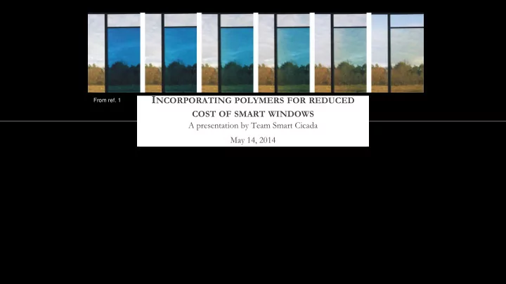
From ref. 1
I NCORPORATING POLYMERS FOR REDUCED From ref. 1 COST OF SMART - - PowerPoint PPT Presentation
I NCORPORATING POLYMERS FOR REDUCED From ref. 1 COST OF SMART WINDOWS A presentation by Team Smart Cicada May 14, 2014 M OTIVATION AND P URPOSE Low eco-impact buildings Smart Window - a solid state device that changes based on
A presentation by Team Smart Cicada May 14, 2014
COST OF SMART WINDOWS
From ref. 1
[2]
layer to cause changes in optical properties
○ ITO/WO3/PEI/Pt-Mg4Ni/ITO ○ Our device replaces ITO with PEDOT:PSS as a conductive transparent electrode and WO3 with PANI as the ion storage layer: ○ PEDOT:PSS/PANI/PEI/Pt-Mg4Ni/PEDOT:PSS
layer is dependent on processing conditions ○ Polymer Synthesis ■ PANI ■ PEI ■ PEDOT:PSS ○ Deposition Methods ■ Spin Coating ■ Meyer Rod Coating
○ Mg4Ni layer on PEDOT:PSS ■ Goal of 70nm of Mg4Ni ■ Power ratio of 1.88 : 1 for Mg : Ni ■ Absorbing and desorbing hydrogen ○ Pt layer on Mg4Ni layer ■ Goal of 4nm of Pt ■ Shiny and like mirror ■ Protect the film from oxidation
AJA Sputtering unit
○ One layer is rate limiting ○ Most likely MgH2/MgNiH4 or PANI ○ Assume dimensions for
prototype and dielectric ○ Use data from literature to assess conductivity
8 /ohm-m
W
○ Included Wave Optics Module
○ Model transmittance and reflectance vs. wavelength/frequency ○ Could do this for a simple 2-layer, 3-D model ■ More advanced models proved to be difficult ■ Computing issues / Frequency sweep issues
○ Model transmitted light beam intensity through our device ○ Simple 2-D model with accurate layer thicknesses ○ Frequency Domain, time independent, FEM
choices in COMSOL.
experimental constants
From left to right: concentrated PANI, PEDOT:PSS, and PEI solutions
Uneven Coating Preliminary Spin Coating Attempts
Meyer Rod Spin Coating Drop Casting
Delicate Film Multiple Layers Split Final Deposition Techniques
Preliminary Spin Coating Attempts Final Deposition Techniques Rough, Uneven Coating, Agglomerations Too thin vs. Too rough, too thick
Spin Coating Drop Casting
Pt on Mg4Ni PEDOT:PSS PEI PANI Glass
Profilometer Tenco Alpha Step 200
○ PANI layer by spin-coating - 70nm ○ PANI layer by drop-casting - 4um ○ PEDOT layer - 70 nm ○ PEI layer - 70nm ○ Mg4Ni layer & Pt layer - 200nm
○ PANI layer by spin-coating - 70nm ○ PANI layer by drop-casting - 4um ○ PEDOT:PSS layer - 70 nm ○ PEI layer - 70nm ○ Mg4Ni layer & Pt layer - 200nm
Clockwise from top left, PANI by spin-coating, PEDOT:PSS, PANI by drop-casting, and PEI.
N&K spectrophotometer a
○ PEDOT:PSS layer ■ 1.68 as refractive index ■ About 94% as reflectivity @ 900nm ○ PEI layer ■ 1.62 as refractive index ■ About 92% as reflectivity @ 900nm
○ PEDOT:PSS layer ■ 1.68 as refractive index ■ About 94% as reflectivity @ 900nm ○ PEI layer ■ 1.62 as refractive index ■ About 92% as reflectivity @ 900nm
Clockwise from top left, index of refraction and reflectivity of PEDOT:PSS and reflectivity and index of refraction of PEI layer.
Final prototype showing hydrogenated Mg4Ni (above) compared to its reflective state (below)
○
modelling ○ N-and-K Spectrometry ○ More techniques and equations ○ Mechanism of hydrogen diffusion for electrical modelling
○ Deposit thicker PEI ○ Thinner Mg4Ni ○ Smoother PANI
Optical Analysis
Electrical Analysis
Xin Zhang Sean Fackler
the Fablab staff the rest of the Materials Science Department faculty and staff and YOU, our supporters :D
1. Baetens R, Jelle BP, and A Gustaven. “Properties, requirements and possibilities of smart windows for dynamic daylight and solar energy control in buildings: A state-of-the-art review.” Solar Energy Materials and Solar Cells, vol. 94; pp.87-105. 2010. 2. Tajima K, Hotta H et al. “Electrochromic switchable mirror glass fabricated using adhesive electrolyte layer.” Applied Physics Letters, vol. 101. 2012. 3. Kirchmeyer S and K Reuter. “Scientific importance, properties, and growing applications of poly(3,4-ethylenedioxythiophene).” Journal of Materials Chemistry, vol. 15; pp. 2077-88. 2005. 4. Deepa M, Ahmad S, et al. “Electrochromic properties of polyaniline thin film nanostructures derived from solutions of ionic liquid/polyethylene glycol.” Electrochimica Acta, vol. 52; pp. 7453-63. 2007.
glasswares and a spin-coater machine to synthesize polymer.
deposition equipment.
fabricate the Mg4Ni/Pt.
layer of Mg4Ni/Pt.
ellipsometer to measure indices of refraction for each layer.
profilometer to characterize to find out the thickness of each layer exactly.
spectrometer to characterize under various applied voltages.
Multiphysics 4.4 to set proper models up.
electrical properties requires a variety of machines. FACILITIES
transparent to absorbing under stimulus
thereby maximize building energy efficiency
reflective smart window, better for deterring radiative heating
limit financial viability
costs while maintaining effectiveness of the switchable mirror
From SwitchLite website: http://www.switchlite.com/home.html#
human health concern
properly
temperature
dangerous
improvement of sustainable building design