+ + + Fig.2- Ionic Liquid Penetration inside layers Fig.1- OPV - - PowerPoint PPT Presentation

fig 2 ionic liquid penetration inside layers fig 1 opv
SMART_READER_LITE
LIVE PREVIEW

+ + + Fig.2- Ionic Liquid Penetration inside layers Fig.1- OPV - - PowerPoint PPT Presentation

Num umeric ical l mode odell llin ing of of ion onic ically ly gated sm smal all mole olecule le OPV V stru tructure Abolfazl Mahmoodpoor 1 , Pavel Voroshilov 1 and Anvar Zakhidov 1,2 1 Department of Physics and Engineering, ITMO


slide-1
SLIDE 1

Abolfazl Mahmoodpoor1, Pavel Voroshilov1 and Anvar Zakhidov1,2

Num umeric ical l mode

  • dell

llin ing of

  • f ion
  • nic

ically ly gated sm smal all mole

  • lecule

le OPV V stru tructure

1 Department of Physics and Engineering, ITMO University, Saint Petersburg 197101, Russia 2 Physics Department and The NanoTech Institute, The University of Texas at Dallas, Richardson 75080, USA

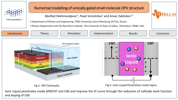
Introduction Theory Simulation Implementation Results Conclusion Fig.1- OPV Schematic Fig.2- Ionic Liquid Penetration inside layers

Ionic Liquid

_ _ _

+

+ + +

+ +

  • CNT

CNT

Ionic Liquid penetrates inside MWCNT and C60 and improve the IV curve through the reduction of cathode work function and doping of C60

slide-2
SLIDE 2

Abolfazl Mahmoodpoor, Pavel Voroshilov and Anvar Zakhidov

Numeric ical modell llin ing of

  • f ion

ionic icall lly gated ed small mol

  • lecule

le OPV str tructure

Introduction Theory Simulation Results Conclusion

Electrical Part → Drift Diffusion Model Grove, A. S. Physics and Technology of Semiconductor Devices; John Wiley & Sons, Inc., 1967. Optical part → Transfer Matrix Method Main system of equation Boundary Conditions

Implementation

[1] Koster, L. J.; Smits, E.; Mihailetchi, V.; Blom, P. Device model for the operation of polymer/fullerene bulk heterojunction solar cells. Physical Review B2005, 72, 085205. [2] Grove, A. S. Physics and Technology

  • f

Semiconductor Devices; John Wiley & Sons, Inc., 1967.

slide-3
SLIDE 3

Numeric ical modell llin ing of

  • f ion

ionic icall lly gated ed small mol

  • lecule

le OPV str tructure

Introduction Theory Simulation Implementation Results Conclusion

Recombination → Langevin recombination local disorder in polymeric materials the dissociation rate is integrated over a Gaussian distribution of separation distances Excitons Generation → Onsager-Braun theory

[3] Mingebach, M.; Walter, S.; Dyakonov, V.; Deibel, C. Direct and charge transfer state mediated photogeneration in polymer-fullerene bulk heterojunction solar cells.Appl. Phys. Lett2012, 100 [4] Barker, A.; Ramsdale, C. M. Modeling the current-voltage characteristics of bilayer polymer photovoltaic devices.Phys. Rev. B2003, 67 [5] Langevin, P. Recombinaison et mobilites des ions dans les gaz. Ann.

  • Chim. Phys.1903,

28, 433–530.

Abolfazl Mahmoodpoor, Pavel Voroshilov and Anvar Zakhidov

for considering local disorder in

  • rganic

material the dissociation rate is integrated over a Gaussian distribution of binding distances

slide-4
SLIDE 4

Numeric ical modell llin ing of

  • f ion

ionic icall lly gated ed small mol

  • lecule

le OPV str tructure

Introduction Theory Simulation Results Conclusion

Energy Diagram of OPV Simulation Parameters We used finite element method and simulated OPV in one dimension

Implementation

Abolfazl Mahmoodpoor, Pavel Voroshilov and Anvar Zakhidov

Fig.3- Energy diagram of OPV

slide-5
SLIDE 5

Numeric ical modell llin ing of

  • f ion

ionic icall lly gated ed small mol

  • lecule

le OPV str tructure

Introduction Theory Simulation Implementation Results Conclusion

We changed the barrier and defined dopant concentration and profile, and used the generation rate from optical part

Fig.4- Electric field distribution in OPV Fig.5- Generation Rate Fig.6- Dopant Concentration in C60 layer

[6] Torben Menke, Debdutta Ray, Hans Kleemann, Karl Leo and Moritz Riede, Determining doping efficiency and mobility from conductivity and Seebeck data

  • f n-doped C60 layers, Basic Solid State Physics, 252(8), 1877–1883

Abolfazl Mahmoodpoor, Pavel Voroshilov and Anvar Zakhidov

slide-6
SLIDE 6

Numeric ical modell llin ing of

  • f ion

ionic icall lly gated ed small mol

  • lecule

le OPV str tructure

Introduction Theory Simulation Results Conclusion Implementation Fig.7- Fitted IV curves for different barrier, different mobility and different dopant concentration Fig.8- Fitted IV curve for 0.14 V barrier and considering different phenomena Fig.9- Mobility changing for different dopant concentration correspond to different gate voltage

Abolfazl Mahmoodpoor, Pavel Voroshilov and Anvar Zakhidov

slide-7
SLIDE 7

Numeric ical modell llin ing of

  • f ion

ionic icall lly gated ed small mol

  • lecule

le OPV str tructure

Introduction Theory Simulation Results Conclusion Implementation Fig.10- Energy diagram of OPV when the gate voltage is 0 V (left) and 2 V (right) at the point of maximum extracted power

Abolfazl Mahmoodpoor, Pavel Voroshilov and Anvar Zakhidov

slide-8
SLIDE 8

Num umeric ical l mode

  • dell

llin ing of

  • f ion
  • nic

ically ly gated sm smal all mole

  • lecule

le OPV V stru tructure

Introduction Theory Simulation Results Conclusion

  • 1. Penetration of dopant from ionic liquid into the cathode raises the Fermi level of the cathode significantly in a

way that the potential barrier between LUMO level of the ETL layer and cathode becomes zero.

  • 2. The dopant penetrates further from the cathode side and reaches the ETL layer affecting the macroscopic

properties of the ETL layer.

  • 3. The dominant phenomena in improving OPV performance using ionic liquid is raising of the cathode Fermi level

and forming an ohmic contact between the ETL layer and cathode. Danila S. Saranin, Abolfazl Mahmoodpoor, Pavel M. Voroshilov, Constantin R. Simovski, and Anvar A. Zakhidov* ,Ionically Gated Small Molecule OPV: Interfacial doping of Charge collector and Transport layer, arXiv:1805.10954. Contacts: * zakhidov@utdallas.edu Abolfazl Mahmoodpoor1, Pavel Voroshilov1 and Anvar Zakhidov1,2

1 Department of Physics and Engineering, ITMO University, Saint Petersburg 197101, Russia 2 Physics Department and The NanoTech Institute, The University of Texas at Dallas, Richardson 75080, USA

Implementation