Electrically tunable trion-polaritons in MoSe 2 heterostructures V. - - PowerPoint PPT Presentation

electrically tunable trion polaritons in mose 2
SMART_READER_LITE
LIVE PREVIEW

Electrically tunable trion-polaritons in MoSe 2 heterostructures V. - - PowerPoint PPT Presentation

Electrically tunable trion-polaritons in MoSe 2 heterostructures V. Kondratyev 1 , E.Khestanova 1 , V. Kravtsov 1 ,T.Ivanova 1 ,F.Benimetskiy 1 , A.Samusev 1 ,I. Iorsh 1 1 Department of Physics and Engineering, ITMO University, St.


slide-1
SLIDE 1
  • V. Kondratyev1, E.Khestanova1, V. Kravtsov1,T.Ivanova1,F.Benimetskiy1, A.Samusev1 ,I. Iorsh1

1Department of Physics and Engineering, ITMO University, St. Petersburg,197101, Russia

Electrically tunable trion-polaritons in MoSe2 heterostructures

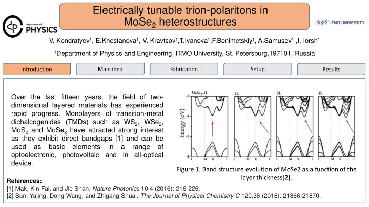
Introduction Main idea Fabrication Setup Results References: [1] Mak, Kin Fai, and Jie Shan. Nature Photonics 10.4 (2016): 216-226. [2] Sun, Yajing, Dong Wang, and Zhigang Shuai. The Journal of Physical Chemistry C 120.38 (2016): 21866-21870.

Over the last fifteen years, the field of two- dimensional layered materials has experienced rapid progress. Monolayers of transition-metal dichalcogenides (TMDs) such as WS2, WSe2, MoS2 and MoSe2 have attracted strong interest as they exhibit direct bandgaps [1] and can be used as basic elements in a range

  • f
  • ptoelectronic,

photovoltaic and in all-optical device. Figure 1. Band structure evolution of MoSe2 as a function of the layer thickness[2].

slide-2
SLIDE 2
  • V. Kondratyev1, E.Khestanova1, V. Kravtsov1,T.Ivanova1,F.Benimetskiy1, A.Samusev1 ,I. Iorsh1

Introduction Main idea Fabrication Setup Results

Scheme of proposed device Motivation The optical properties of TMDs are defined by the formation of bound electro neutral excitonic (X0) and charged trionic (X−

  • r

X+) states, which are characterized by the large binding energies on the order

  • f 100 meV and an increased oscillator strength [3].

Trions are charged particles which makes them highly electrically tunable and promising for the engineering of electro-optical devices. In the present work, we realize the concept of electrically-driven trion-polaritons and demonstrate the electrically tunable polariton gap.

References: [3] Wang, Haining, et al. "Physical Review B 93.4 (2016): 045407.

Electrically tunable trion-polaritons in MoSe2 heterostructures

slide-3
SLIDE 3
  • V. Kondratyev1, E.Khestanova1, V. Kravtsov1,T.Ivanova1,F.Benimetskiy1, A.Samusev1 ,I. Iorsh1

Electrically Tunable Trion-polaritons in MoSe2 Heterostructures

Introduction Main idea Fabrication Setup Results

Sample Methods

We engineered a photonic structure consisting

  • f a MoSe2/hBN heterostructure placed on top
  • f Ta2O5 grating. To create a proper contact to

MoSe2, electron beam lithography through a polymethyl acrylate mask. During the lithographic process, the areas for contact were

  • pened in the mask layer and Ti/Au metal

contacts were deposited using thermal

  • evaporation. We chose Ti as an adhesive layer

because of its work function (4.3 eV) being close to the electron affinity of MoSe2 (3.8 eV) and hence should promote a low Schottky barrier at the metal/semiconductor contact. The electrical tuning of the device consists of the application

  • f

a vertical field (gate) which changes the Fermi level of the monolayer MoSe2 and thus the concentration of trions.

Ta2O5 MoSe2 hBN Contact

  • 300
  • 200
  • 100

100 200 300 1.58 1.60 1.62 1.64 1.66 V sample (V) Energy (eV)

X0 X-

max min

  • Fig2. (a)Optical microscopy image of fabricated sample.

(b) Plot of photoluminescence (PL) spectra versus gate voltage. PL intensity

slide-4
SLIDE 4
  • V. Kondratyev1, E.Khestanova1, V. Kravtsov1,T.Ivanova1,F.Benimetskiy1, A.Samusev1 ,I. Iorsh1

Electrically Tunable Trion-polaritons in MoSe2 Heterostructures

Introduction Main idea Fabrication Setup Results

Setup for microphotoluminescence spectroscopy in Fourier plane imaging configuration.

We characterize the gate dependence of the total photoluminescence of our device. For this, we employ a setup which contains a closed-cycle helium cryostat with a base temperature of 7K. To excite photoluminescence we use He-Ne laser with a wavelength of 632.8 nm. The beam was focused

  • n

a sample by an

  • bjective

lens (Mitutoyo Objective 100x/0.7). The collected photoluminescence signal was directed to the slit spectrometer (Princeton SP2500, CCD camera PyLoN 400BReXcelon). To excite our sample electrically KEITHLEY Model 6487 was used, the voltage was applied to monolayer, ground to Si, to prevent the insulator breakdown we used built-in current compliance.

  • Fig3. Setup scheme
slide-5
SLIDE 5
  • V. Kondratyev1, E.Khestanova1, V. Kravtsov1,T.Ivanova1,F.Benimetskiy1, A.Samusev1 ,I. Iorsh1

Electrically Tunable Trion-polaritons in MoSe2 Heterostructures

Introduction Main idea Fabrication Setup Results

75V 0V 200V Au/Cr

Si SiO2 hBN Ta2O5 MoSe2

V

Fig4.(a) Scheme of device. (b)-(d) Angle-resolved reflectance spectra of the hybrid sample for different gate voltages.

a) c) b) d) X0 X0 X- X- X0 X- X0 X- X- X0 To observe trion-polaritons we investigate the angular dependence of the reflectance from our structure. For this, we use the setup for spectromicroscopy in Fourier plane imaging configuration. In the reflectance maps shown in Fig.4(d) it is clearly seen that at V = 0 V only excitonic polariton gap exists, while at V = 75 V a trion-polariton emerges. X0 This results show that we have experimentally demonstrated electrically-tunable trion-polartion in planar optical cavity.