ECS CSEL EL Bro roker erage age Event nt 2016 16 ECSE CSEL - - PowerPoint PPT Presentation

ecs csel el bro roker erage age
SMART_READER_LITE
LIVE PREVIEW

ECS CSEL EL Bro roker erage age Event nt 2016 16 ECSE CSEL - - PowerPoint PPT Presentation

ECS CSEL EL Bro roker erage age Event nt 2016 16 ECSE CSEL Joint Undertak aking ng Nano-Imprint Lithography Large Surface Pilot Line RIA Proposal Anneliese Pnninger Courtesy of Fraunhofer ISE a.poenninger@evgroup.com NIL


slide-1
SLIDE 1

ECS CSEL EL Bro roker erage age Event nt 2016 16

ECSE CSEL

Joint Undertak aking ng

Anneliese Pönninger a.poenninger@evgroup.com

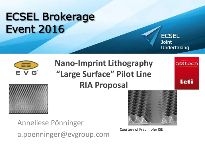
Nano-Imprint Lithography “Large Surface” Pilot Line RIA Proposal

Courtesy of Fraunhofer ISE

slide-2
SLIDE 2

ECSEL SEL Brok

  • ker

erage ge Event nt 2016

NIL –Why and What for?

2

  • More than Silicon substrates

(Polymer/Flexible/Sapphire...)

  • High resolution / Large surface
  • High throughput
  • Bio compatible polymers
  • Polymer

for permanent applications

  • 3D complex shapes
  • Non flat samples

MEMS NEMS Image Sensors Displays Solar Cells BioMEMS Flexible e- OLED LED Micro Fluidics Plasmonic Components

slide-3
SLIDE 3

ECSEL SEL Brok

  • ker

erage ge Event nt 2016

3

Solutions Transferred to End Users or Companies in the value chain. Market Needs End User Request (design / product) NIL Value Chain (Master, Equipment, Material, Metrology, Integration) Pilot Line Environment (infrastructure building, solution qualification and integration)

NIL – Project Concept

slide-4
SLIDE 4

ECSEL SEL Brok

  • ker

erage ge Event nt 2016

A little more technical information about my project

4

  • Standardization w.r.t. applications
  • Fully automated solutions assessed in pilot line environment
  • what about real alignment capabilities in production regime?
  • what about the real defectivity levels and what are the real bottlenecks?
  • Associated metrology (real time is not needed for wafer scale, but in line YES!)
  • Defectivity assessment w.r.t. applications
  • “Real” CoO assessment in pilot line in a full process flow (yield, stamp lifetime…).
  • Validation of some “elementary modules” that are still missing in the value chain:

Stamp Design (w.r.t. process that will be implemented), Stamp Repair, Complete Simulation ToolBox.

Demonstrate Industrial Maturity Qualify a well established Supply chain

slide-5
SLIDE 5

ECSEL SEL Brok

  • ker

erage ge Event nt 2016

Information about the Consortium

  • Consortium under construction / RIA call / Total budget 15 M€
  • NIL technology maturity TRL from 4 (start) to 6 (in 2019)
  • Materials development, metrology
  • Device design and manufacturers

– Photonics (LED, displays, opto-electronics) – Bio-technology – MEMS, Flexible support, @ wafer level / @ large surface scale level etc.

  • End-user assessment / Specific Work packages // NIL options.

5

To accelerate adoption of this technology. To demonstrate the benefits of the full-wafer NIL technology and spreading its use for applications beyond the traditional semiconductor industry.

slide-6
SLIDE 6

ECSEL SEL Brok

  • ker

erage ge Event nt 2016

Thank you!

Anneliese Pönninger A.Poenninger@EVGroup.com, EV Group

DI Erich Thallner Str. 1, 4782 St. Florian am Inn, Austria

www.EVGroup.com

6