Chapter 2 Chapter 2 Electronics In In Out Out In Out The - - PowerPoint PPT Presentation

chapter 2 chapter 2
SMART_READER_LITE
LIVE PREVIEW

Chapter 2 Chapter 2 Electronics In In Out Out In Out The - - PowerPoint PPT Presentation

Digital IC-Design An Inverter in Different Views Logic V DD Design Digital Chapter 2 Chapter 2 Electronics In In Out Out In Out The Manufacturing UV light Lithographic Optical mask Process GND Layout Process Process Photo


slide-1
SLIDE 1

1

Chapter 2

Digital IC-Design

Chapter 2 The Manufacturing Process Process
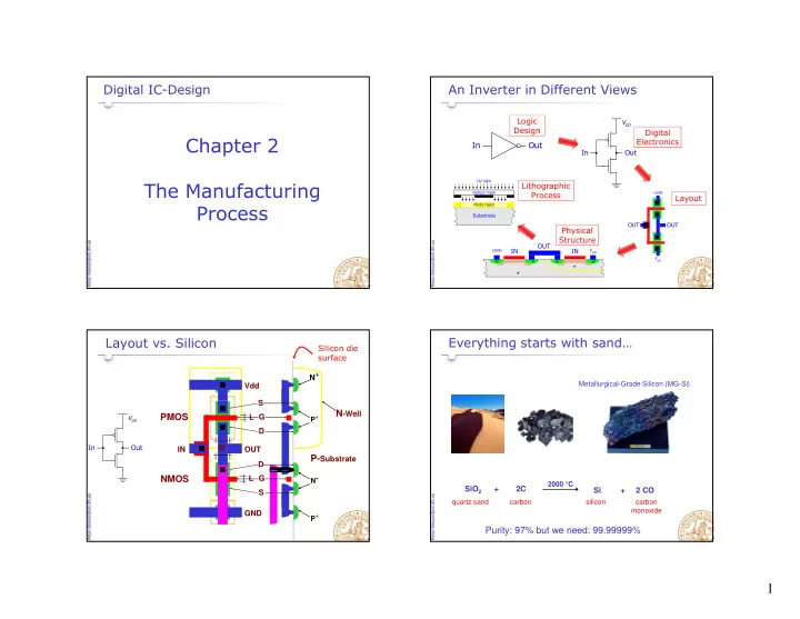
Logic Design

An Inverter in Different Views

Out In

VDD

Digital Electronics Out In

Out In

Substrate

UV light Photo resist Optical mask

Lithographic Process

GND

Layout

p-

OUT

VDD

n+ n+ p+ p+ n-

GND

IN IN

Physical Structure

OUT

VDD

OUT

Layout vs. Silicon

N+ Vdd S Silicon die surface

N-Well P-Substrate

P+

PMOS

W L IN OUT S G D D

Out

VDD

In P+ N+

NMOS

L GND G S

Everything starts with sand…

Metallurgical-Grade Silicon (MG-Si)

SiO2 + 2C

2000 °C

Si + 2 CO

quartz sand carbon carbon monoxide silicon

Purity: 97% but we need: 99.99999%

slide-2
SLIDE 2

2

Fabrication

Oxiation Masking/Patterning Etching

Wafer Processing Si - Ingot Si - Wafers Processed wafer Die Attach Wire Bonding Encapsulated IC

Manufacturing: A Lithographic Process Photographic glass plate (mask) Each layer is projected to the silicon die Manufacturing Process: Example

Substrate

Etching Resist SiO2

Substrate Substrate (Si)

Photo resist Silicon dioxide (SiO2) UV light Si After etching & resist removal Resist SiO2 Si Exposed resist UV light Resist Optical mask SiO2 Si Implant of heavily doped areas SiO2 Si

Manufacturing Process: Simplified Implantation of well regions D it l ili Deposit polysilicon

  • Gate

Implantation of heavy doped regions

  • for Drain, source, and substrate/well contacts

Creating windows for contacts and Creating windows for contacts and vias Deposit metal

slide-3
SLIDE 3

3 Wafer

Each mask is repeated with a stepper Intel use 30cm wafers in 90nm technology

Reticule

For us: MPW - many designs share the same reticule Silicon dies (chips) after die i sawing

Wafer Stepper

Light goes through the mask, lens and the objective

mask

the objective

lens

  • bjective

wafer

Optical Mask Feature sizes are close to light wave lengths Diffraction phenomena have become a major problem

Out of reach for the Out of reach for the Optics!!! Mask correction is needed!

Optical Proximity Correction (OPC)

Predistortion of the mask layout is needed when scaling down the technology

OPC Corrections

With OPC No OPC

OPC Corrections Original Layout

Needed for 0.1 micron and less

slide-4
SLIDE 4

4

Phase Shifting Masks (PSM)

conventional mask

glass

phase shifting mask

Phase shifter (glass)

To much light for the photo resist

OK!

Clean room

To keep the air clean of particles

Clean Room Particles in the air

  • air in a city:

15 million -100 million particles per ft3

  • air in the mountains:

up to 10 million particles per ft3 ft3

  • air in a clean room for ICs:

1 - 100 particles per ft3

Digital IC-Design

Design Rules

slide-5
SLIDE 5

5

Design Rules

Interface between designer and process Interface between designer and process engineer Guidelines for constructing process masks Unit dimension: Minimum line width scalable design rules: λ parameter scalable design rules: λ-parameter absolute dimensions (micron rules)

Layer Representation

Well A ti Polysilicon Contact to poly Metal 2 Metal 1 Active Contact to poly Contact to active Via (M1 to M2)

Minimum Distance Rule (typ. 0.35 tech.) Active Poly M1 M1

M2

0.6μm 0.6μm 0.6μm 0.6μm Minimum Width Rule (typical 0.35 tech) Active Poly M1 M1

M2

0.5μm 0.5μm 0.4μm 0.3μm

slide-6
SLIDE 6

6

Transistor Rules (0.35 technology)

0.3μm 0 4μm 0.6μm 0 7 m 0 7 m 0.3μm 0.4μm μ 0.7μm 0.7μm

Note that the minimum transistor width is wider than the minimum active width (0.5μm)

0.6μm 0.4μm 0.5μm

Contact Rules (0.35 technology)

Contacts have fixed size (0.42)

0.6μm 1.0μm 0.4μm 1.0μm 0.5μm 0.4μm 0.4μm

( )

0.7μm 0.9μm 0.5μm

Contact to active Contact to poly Via (Metal 1 to Metal 2)

Layout Editor Design Rule Checker (DRC) Polysilicon to y close to active!

slide-7
SLIDE 7

7

Packaging Packaging follows after fabrication Bonding Pads Core Bonding wire Pads Core Silicon die

Bonding on the border around the core

Flip-Chip Bonding

Die upside down Solder Bumps Die upside down

Die

Inter- connect layer Bonding everywhere even inside the core

Substrate

Some Package Types

DIP

Dual in line Package

Bonded Silicon Die Wafer PGA

Pin Grid

PLCC

Array

Packages add Parasitics

Package Capacitance (pF) Inductance (nH) Package Capacitance (pF) Inductance (nH) 68 Pin Plastic DIP 4 35 68 Pin Ceramic DIP 7 20 256 Pin Grid Array 5 15 Bond Wire 1 1 Solder Bump 0 5 0 1 Solder Bump 0.5 0.1

Source: Sze