
SLIDE 1
Modern Semiconductor Devices for Integrated Circuits (C. Hu) Slide 1-1
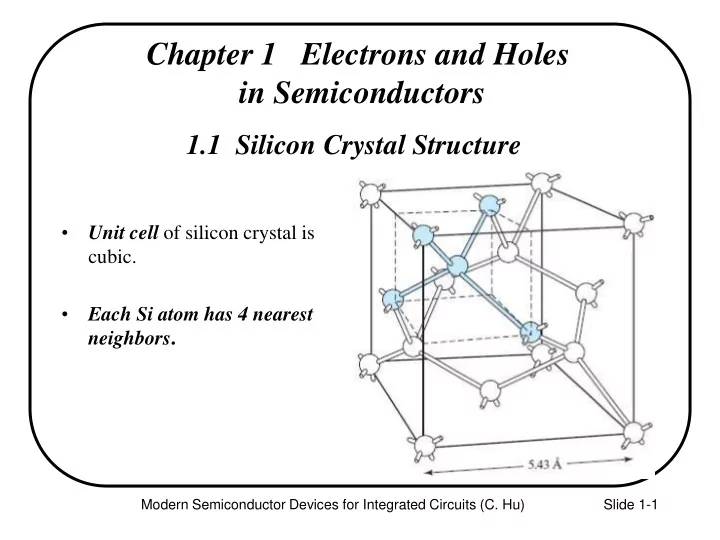
1.1 Silicon Crystal Structure
- Unit cell of silicon crystal is
cubic.
- Each Si atom has 4 nearest
neighbors.