SLIDE 1 Part I
Automotive Systems
1 051214 Eyad Alkassar Introduction
ECU1 ECUn bus
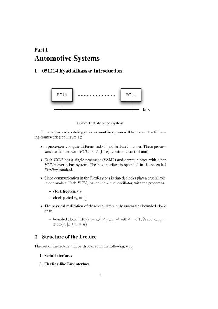
Figure 1: Distributed System Our analysis and modeling of an automotive system will be done in the follow- ing framework (see Figure 1):
- n processors compute different tasks in a distributed manner. These proces-
sors are denoted with ECUu, u ∈ [1 : n] (electronic control unit)
- Each ECU has a single processor (VAMP) and communicates with other
ECUs over a bus system. The bus interface is specified in the so called FlexRay standard.
- Since communication in the FlexRay bus is timed, clocks play a crucial role
in our models. Each ECUu has an individual oscillator, with the properties – clock frequency ν – clock period τu =
1 νu
- The physical realization of these oscillators only guarantees bounded clock
drift: – bounded clock drift: (τu −τu′) ≤ τmax ·δ with δ = 0.15% and τmax = max{τu|1 ≤ u ≤ n}
2 Structure of the Lecture
The rest of the lecture will be structured in the following way:
- 1. Serial interfaces
- 2. FlexRay-like Bus interface
1
SLIDE 2
- construction
- integration with processors
- 3. WCET: worst case execution time
- Based on WCET analysis we will show theorems of the following
form: Having knowledge about the concrete C-program P, the used compiler, the underlying hardware it holds that i) P is correct ii) P ter- minates in less than T cycles.
- The analysis of WCET is based on techniques from the UdS Spin-Off
- AbsInt. This analysis is based not only on the considered code in As-
sembler or C, but also on the gate-level implementation of the proces- sor.
- 4. OLOS: OSEK-time like OS
In this chapter we will build upon the hardware and FlexRay model an Op- erating System called OLOS (OLOS is a dialect of Communicating Virtual Machines or in short CVM. CVM implements the basic functionality of a µ- kernel). The Operating System is running on each ECU and provides task abstraction and communication primitives. Furthermore it implements the drivers for the FlexRay interfaces.
- 5. D-OLOS: distributed OLOS
In this chapter we will connect many different ECUs with OLOS running
- n top of them. This will provide us with the complete programming level
- f the user.
3 Serial Interfaces
3.1 Some formal stuff
We will use the following notations (where a, b ∈ Z):
- [a : b] = {a, a + 1, . . . , b}
- [a : b) = [a : b − 1],
(a : b) = [a + 1 : b − 1], (a : b] = [a + 1 : b].
- c + [a : b] = [a : b] + c = [a + c : b + c]
- We model time as the set of real numbers: time = R+
2
SLIDE 3
- A signal is a mapping from time to the values 0, 1 or Ω (which denotes an
unknown value). time → {0, 1, Ω} The content on the bus is written into the register, whenever the clock signal is set to one. Clocks to the registers are modeled in the following way:
- A clock is modeled as function, mapping time to boolean values, i.e. ck :
time → {0, 1}
- A clock oscillates between the values 1 and 0. The ith time it changes it
value from 0 to 1 (this position in time is called raising edge, the whole period between two raising edges is called cycle) is e(i) = α + i · τ with i ∈ N0, where α is some offset value of the clock.
- With that we can define: ck(t) ≡ ∃i : t ∈ [e(i) : e(i) + τ/2]
τ/2 e(i) e(i+1) th ts ce
Figure 2: Holding and Setup time for a register reading from the bus on a raising edge We have two operating conditions for a register at every raising edge e(i) when some data is sampled: 1) the clock enable signal must stay stable and 2) if it is set to 1 (i.e. updating) the input signal must stay stable:
- Clock enable stable ∃y ∈ {0, 1} ∀t ∈ (e(i) + [−ts, th]) : ce(t) = y, where
y denotes whether there should be an update or not. ts and th stand for setup and hold time (see Figure 2). The period e(i) + [−ts, th] is called sampling interval.
- Data input stable Let B : time → {0, 1, Ω} be some input signal. If for the
whole sampling interval the clock enable signal stays stable then it holds: ∃x ∈ {0, 1} ∀t ∈ (e(i) + [−ts, th]) : B(t) = x. Next we define the value a register holds at time t between two raising edges e(i) and e(i + 1). There are three periods (see Figure 3). In the first period the 3
SLIDE 4 e(i) tpmin B R
Ω x y
tpmax
x Figure 3: The content of the Register when reading from the bus at edge e(i) content of the register stays the old one (before the first raising edge). Then it follows a period where the value is flipping and is therefore undefined. This period lasts from e(i)+tpmin to e(i)+tpmax. Finally the Register holds the input value x: ∀t ∈ (e(i) : e(i + 1)] if ce(t) = 1 then R(t) = R(e(i)) : t ∈ e(i) + (0 : tpmin] Ω : : t ∈ e(i) + (tpmin : tpmax) x : : t ∈ [e(i) + tpmax : e(i + 1)] We define the value Ri to be the content of Register R at the end of cycle i, i.e. Ri = R(e(i + 1)). If the second operating condition of a register is violeted, i.e. the input data is not stable during the sampling interval of edge i, it could happen (with small probability) that the content of the register is undefined even after e(i)+tpmax. This phenomenon is called meta stability. To avoid meta stability we read the content of the first Register into a second one, called
R is clocked as the first one. By that construction (see Figure 4) we lower the probability that R is meta stable after e(i) + tpmax (from p for register R to, p2 for R), i.e. it practically holds: ∀i : ∃ x ∈ {0, 1} : ∀t ∈ (e(i) + tpmax, e(i + 1) + tpmin] : R(t) = x This only holds if tpmin is greater or equal to the Register holding time. Else the second operating condition would be violated for Register R. 4
SLIDE 5
S R R^ 1 1 ckr cks
Figure 4: Bus link structure of Sender (S) and Receiver(R) 5
SLIDE 6 4 051219 Sebastian Bogan FlexRay Bus interface
Register
R Rin R ck ce
Ri+1 =
in
: ci
e = 1
Ri : otherwise Figure 5: Register R Gates
b a c
g ∈ {∧, ∨, . . .}, ci = g(ai, bi) Figure 6: Gate g Open Collector Outputs
VCC GND R1 R2
1 : R1 low ∧ R2 high : R1 high ∧ R2 low highZ : R1 high ∧ R2 high Figure 7: Open Collector 6
SLIDE 7 VCC GND pullup resistor R2
1 : R2 high : R2 low Figure 8: Pullup Resistor We define the value of the Bus B at time t as conjunction over all sender values. B(t) = S(t) ∧ . . . ∧ S′(t) With 0 ∧ Ω = 0, Ω ∧ 1 = 1, 1 ∧ Ω = 1, Ω ∧ Ω = Ω, Ω ∧ 0 = 0 We define the content of the registers R (connected to bus B) and ˆ R at the time er(j) as follows (Figure 4). Rj = B(er(j)) : B(t) = B(er(j)) ∀t ∈ er(j) + [−ts, th] Ω : otherwise ˆ Rj = Rj−1 : Rj−1 ∈ {0, 1} x ∈ {0, 1} : otherwise Affected Cycles Assume a sender puts a new value on the bus at time es(i). Then for all receiver edges er(j) such that er(j)+th ≤ es(i) sampling is not affected by this new value (not considering propagation delays).
er(j) es(i) ts th
Figure 9: Not affected sampling Definition 4.1 cy(i) is the index of the first receiver edge, that is affected by es(i). cy(i) = min{j | er(j) + th > es(i)} 7
SLIDE 8 That means, that a receiver edge j is affected by a sender edge i if it is in the region (es(i) − th, es(i) − th + τr]. j = cy(i) = ⇒ es(i) − th < er(j) ≤ es(i) − th + τr The formula above could as well be written as: j = cy(i) = ⇒ es(i) − th < er(j) ∧ er(j − 1) ≤ es(i) − th
j = cy(i) = ⇒ er(j − 1) ≤ es(i) − th < er(j) From the FlexRay standard we know, the sender puts all bits 8 times on the bus, e.g.: ci−1
es
= 1 ∧ ci
es . . . ci+7 es
= 0 = ⇒ ∀t ∈ [es(i) + tp-max, es(i + 7)] : B(t) = Si That means the receiver samples Si during at least 7 consecutive cycles. Lemma 4.1 7 consecutive cycles Rcy(i)+β+k = Si where k ∈ [0 : 6] β = if er(cy(i)) ≥ es(i) + tp-max + ts 1
Proof. All sampling intervals of all receiver edges cy(i)+k +β are in the region
- f the time where the bus is stable. Both for β = 0 and β = 1.
β = 0: er(cy(i)) + 6τr + th ≤ es(i) − th + τr + 6τr + th (Definition 4.1) = es(i) + 7τr < es(i) + 8τs (bounded clock drift) β = 1: er(cy(i)) + 7τr + th < es(i) + tp-max + ts + 7τr + th (Definition β) ≤ es(i) + τmax(1/2 + 1/10 + 7 + 1/10) (Definition tp-max, ts, th) = es(i) + 7.7τmax < es(i) + 8τs (bounded clock drift) 8
SLIDE 9 τs/2 es(i) es(i+1) th ( ] τ th τr/2 cks ckr τr
Figure 10: A situation where the same sent value affects the receiver in two cycles
5 051221 Matthias Daum
Lemma 5.1 Values that were put on the bus at consecutive sender cycles are usu- ally sampled at consecutive receiver cycles. More precisely,
- 1. cy(i + 1) ∈ [cy(i) : cy(i) + 2]
- 2. If cy(i + 1) = cy(i) + 1, then cy(i + 1 + k) = cy(i + 1) + k for all
k ∈ [0 : 600].1 Proof. Both statements of the lemma are strongly related, hence we show both
Case distinction. At first, we consider the case that τr ≤ τs. The other case, τr > τs, is left for an exercise. We define ∆τ = τs − τr and a = cy(i). Now, we have to find out, under which circumstances cy(i + 1) is not equal to cy(i) + 1. Such a situation is depicted in Figure 10: The sender puts a new value on the bus at time es(i) and the receiver had its rising edge immediately after es(i)−th. Hence, the receiver will be affected by the sender in this cycle. However, the sampling interval in the next receiver cycle will already be over before the sender’s next cycle starts. Consequently, the receiver will again sample the old value and the new value on its next cycle, i.e. cy(i + 1) = cy(i) + 2. Apparently, we experience this situation whenever er(a) ≤ es(i) − th + ∆τ. Case distinction. Case 1: er(a) ≤ es(i) − th + ∆τ
1Assuming a δ ≤ 0.15%. Was corrected later to k ≤ 300 for the new δ ≤ 0.30%.
9
SLIDE 10 = ⇒ er(a) + τr ≤ es(i) − th + ∆τ + τr = es(i) − th + τs − τr + τr = ⇒ er(a + 1) ≤ es(i) − th + τs = es(i + 1) − th And from es(i) − th < er(a) it follows that er(a) + 2τr > es(i) − th + 2τr = es(i) − th + τs + τr − ∆τ = es(i + 1) − th + τr − ∆τ
= ⇒ er(a + 2) > es(i + 1) − th We have just shown that er(a + 1) ≤ es(i + 1) − th < er(a + 2). Hence, the value that was put on the bus at es(i + 1) − th, will be sampled in cycle a + 2, i. e., cy(i + 1) = a + 2 = cy(i) + 2 . Herewith, we have shown that statement 1 holds if τr ≤ τs and er(a) ≤ es(i)− th + ∆τ. Now, we will consider statement 2 of the lemma. We know that es(i) − th < er(a), and hence: er(a) + (1 + k)τr > es(i) − th + (1 + k)τr = es(i) − th + kτs − k∆τ + τr = es(i + k) − th − k∆τ + τr And thus, if k ∆τ ≤ τr, we can conclude er(a + k + 1) > es(i + k) − th We have assumed that er(a) ≤ es(i) − th + ∆τ, hence er(a) + kτr ≤ es(i) − th + ∆τ + kτr = es(i) − th + ∆τ + kτs − k∆τ = es(i + k) − th − (k − 1)∆τ And thus, for k ≥ 1, we can conclude = ⇒ er(a + k) ≤ es(i + k) − th We have just shown that er(a + k) ≤ es(i + k) − th < er(a + k + 1) holds for 1 ≤ k ≤ τr/∆τ. Hence, the value that was put on the bus at es(i + k) − th, will be sampled in cycle a + k + 1, i. e., ∀k.1 ≤ k ≤ τr/∆τ = ⇒ cy(i + k + 1) = a + k + 1 = cy(i) + k + 1 . 10
SLIDE 11 The computation of the numeric upper bound of k is left as an exercise. Case 2: er(a) > es(i) − th + ∆τ As motivated at the beginning of our proof, cy(i + 1) is always cy(i) + 1 in this case: er(a + 1) > es(i) − th + ∆τ + τr (assumption in Case 2) = es(i) − th + τs = es(i + 1) − th er(a) ≤ es(i) − th + τr (Definition 4.1) ≤ es(i) − th + τs (τr ≤ τs) = es(i + 1) − th = ⇒ cy(i + 1) = cy(i) + 1
SLIDE 12 6 060109 Jan D¨
acher
Putting a message m[0 : L−1] on the bus, where m[i] ∈ {0, 1}8 is message byte i. When a message is put on the bus, we have to encode the actual message. In the following, we define the message encoding. At first, we define a few tokens:
- TSS = 0 – Transmission start sequence
- FSS = 1 – Frame start sequence
- BSS[0 : 1] = 10 – Byte start sequence. Note: the transition from 1 to 0
forces so called sync edges on the bus.
- FES = 0 – Frame end sequence
- TES = 1 – Transmission end sequence
We denote the encoded message m by f(m). The encoded message looks as follows: f(m) = TSS ◦ FSS ◦ BSS ◦ m[0] ◦ · · · ◦ BSS ◦ m[L − 1] ◦ FES ◦ TES The length of the encoded message measured in bits is |f(m)| = 4+10·L = n. For the sake of error correction, every bit of the encoded message is transmitted eight times. For some x = x[0 : k − 1] ∈ {0, 1}k, we use the notation 8 · x for x[0]8 ◦ · · · ◦ x[k − 1]8. Thus, in order to deliver the message, we transmit 8 · f(m). On sender side, we expect a y = y[0 : n − 1] ∈ {0, 1}n and y = f(m), especially. Definition 6.1 The predicate onbus(y, γ, τ) is defined as follows: ∀j ∈ [0 : n − 1].∀t ∈ [γ + 8 · τ · j + tpmax : γ + 8 · τ · (j + 1)] : Bt = yj Where y denotes the message f(m), γ the starting point and τ the cycle time of the
- sender. The number of bits in the message is n.
Remark: If the predicate onbus(y, γ, τ) holds, one can assume, that at some sender edge es(i) = γ = αs + τs · i, the message was generated by the flip flop. 12
SLIDE 13 SIO: serial I/O interface On sender side we have a word adressable message send buffer MS (see Fig. 11.
m[0] m[1] m[2] m[3] m[4] m[5] m[6] m[7] 1 Byte fbus Bit
MS(b) = m(4b + 3) ◦ · · · ◦ m(4b) 8 · f(m) = 1 = Bity . . . Bity+8(4+10L) Bitz
ce : z = y − 1, y + 7, y + 8j − 1 for j ≥ 2
Figure 11: Message Send Buffer By means of the address counter in figure 12 we choose the appropriate byte within the word, stored in the message buffer. The address is incremented after the previous byte is transmitted. A byte transmission takes 80 cycles. If a reset signal is triggered, or if AC = L − 1, the counter is reset.
AC λ-inc 1 0 reset v (<AC> = L-1) ce ck
λ = ⌈log L⌉ ACt
ce = 1 ⇔ t = t0 + 80k = tk
for k = 0, . . . , L − 1 AC0
ce = 0
ACt = i ⇔ t ∈ (ti−1 : ti] ACt = 0 ⇔ t < t0 ∨ t > tL−1 Figure 12: Address Counter By means of the byte generation circuit (figure 13) we get the byte which is transmitted later on. We take the 32-bit message out of the message buffer and select the desired byte using multiplexers. 13
SLIDE 14 AC MB 1 0 1 0 1 0 Byte ACce ACce [λ-1:2] [1:2] AC[0] ck ck ck
ACcet = 1 ⇔ t = tk = t0 + 80 · k, with k = 0, . . . , L − 1 ACt = i ⇔ (i = 0 ∧ t ≤ t0) ∨(i > 0 ∧ t ∈ (ti−1, ti]) ∨(i = 0 ∧ t > ti−1) Bytet = mi ⇔ (i < L − 1 ∧ t ∈ (ti−1, ti] ∨(i = L − 1 ∧ t > tL−1) Figure 13: Byte Generation The flex ray controller is controlled by the state automaton depicted in figure 14. The signal start is computed by the circuit in figure 27.
idle TSS Z1 FSS Z2 BSS0 Z3 BSS1 Z4 ...... b7 Z12 FES0 Z13 FES1 Z14 idle Z0 b0 Z5 done start /done
startt = start′t−7 ∨ · · · ∨ start′t donet = (ACt = 0) Figure 14: State Automaton Figure 15 depicts the circuit which is used to determine the bit that should be transmitted.
Byte Bit 0 1 protocol v reset prot1 v reset b[7:0] = Z[12:5] B ACce ck ck Bitce v
prot1 = Z2 ∨ Z3 ∨ Z14 protocol = ¬
l[i] Figure 15: Circuit determines the transmitted bit 14
SLIDE 15 The timing diagram below shows the dependency of the bit which is put on the bus and the current state. We have the constant values 1 and 0, according to the states BSS0 and BSS1, which announce the byte start sequence. Afterwards, the actual bits 0 to 7, of the message, follow in the particular states B0 to B7.
ACce byte Z Bitce Zce Bitin Bit BSS0 BSS1 b0 b7 1 mi,0 mi,7 1 mi,0 mi,7 ti,0 si,1 si,2 si,2 si,0 ti,1 ti,2 ti,3
Bitt = mi,j, t ∈ (Si,j+2, Si,j+3] Bitt = 1, t ∈ (Si,0 : Si,1] Bitt = 0, t ∈ (Si,1 : Si,2] Figure 16: Timing Diagram 1 The clock enable signal bitce for the bit register is computed by the circuit in figure
- 17. Since a bit has to be transmitted 8 times, we update the value of the bit register
- nly after 8 cycles. To count the cycles we use a 3-bit counter.
3-cnt R 1 reset Zce bitce reset cout 3 ck reset
Zce = cout ∨ reset (cout is the overflow bit
bitt
ce = resett ∨coutt−1
Figure 17: Computation of signal bitce 15
SLIDE 16 Figure 18 shows the start period of the transmission. According to the state, de- noted by Z the bit is set to the TSS, FSS, . . . . According to the diagram in figure 18, the predicate
- nbus(f(m), γ, τ), γ ≤ γ0 + (7 + 1) · τ
holds.
start Zce Z
idle TSS FSS BSS0
γ0 r0 r1 r2
r0 = min{t|startt ∧ Zt
ce ≤ γ0 + 7 · τ}
r1 = r0 + 8 r2 = r0 + 16 = t0 Bitt = 0 : t ∈ (r0 + 1, r1 + 1] Bitt = 1 : t ∈ (r1 + 1, r2 + 1] Figure 18: Timing Diagram 2 The end of the transmission is illustrated in figure 19. Here, Bit is set to FES0 and FES1. After the transmission we switch into the idle state.
ACce AC Z Zce b7 FES0 FES1 ti-1 r2' r3' r4' idle ti
r′
3 = r′ 2 + 8
r′
4 = r′ 3 + 8
Bitt = 0 : t ∈ (r′
2 + 1 : r′ 3 + 1]
1 : t ∈ (r′
3 + 1 : r′ 4 + 1]
Figure 19: Timing Diagram 3 16
SLIDE 17 6.1 060111 Sebastian Bogan Receiver Construction
The present section defines the receiver construction. We start off defining the hard-
- ware. Within a series of lemmas we prove the receiver construction. At the end we
prove that an entire message is sampled correctly. 6.1.1 Hardware An n-bit shift register is constructed in the following way.
R R R R ...... ck
1 1 1 1
Rin Rout0 Rout1 Rout2 Rout(n-1)
Rt
= Rt−1
. . . Rt
= Rt−1
Figure 20: n-Bit Shift Register Definition 6.2 An n-bit majority voter realizes the following function. n-major(x[0 : n − 1]) = 1 ⇔| {i | xi = 1} |≥ ⌈n/2⌉ Definition 6.3 The sync signal sync is turned on in cycle t if the decoding state is either idle (Z0) or BSS0 (Z3) and there is a falling edge (Figure 21). An n-bit shift register is constructed in the following way.
R Z0 Z3 sync v 1 ck
synct = (idlet ∨ BSS0t) ∧ (¬vt ∧ vt−1) Figure 21: Sync Definition 6.4 sy(h) denotes the h’th cycle after cy(0), when sync is activated. 17
SLIDE 18 3-cnt sync = 4 strobe
strobe = (cnt = 4)∧¬sync Figure 22: 3-cnt + strobe Definition 6.5 The decoding automaton (Figure 22) is clocked by the strobe sig-
- nal. By means of a 3-bit counter and the sync signal one can define the strobe
- signal. The strobe signal is realized as follows.
Definition 6.6 str(k) denotes the k’th cycle, when strobe is activated after cy(0). Now we assemble all pieces to construct the receiver.
R R^ 5-major 1 v B sh[0:3] 4-shift 8-shift strobe ck ck ck ck
1 1
Figure 23: Hardware Construction Receiver The automaton in figure 24 represents the decoding of a message.
(v=0) ∧ running idle TSS Z1 FSS Z2 BSS0 Z3 BSS1 Z4 ...... b7 Z12 FES0 Z13 FES1 Z14 idle Z0 b0 Z5 v=0 v=1
Figure 24: Decoding Automaton 18
SLIDE 19 6.1.2 Brainware The final proof about correct sampling of an entire message is an inductive proof
- ver sync intervals. The following proof shows, that the initial sync signal (sy(0))
is triggered at cy(0) + [3 : 4]. Lemma 6.1 Initial sync (at transmission start) Assumption: Claim: sy(0) ∈ cy(0) + [3 : 4] Proof. The proof shows, that there is a falling edge between cycle 2 and 3 or between cycles 3 and 4. Hence there is a sync signal cy(0) + [3 : 4]. 0 = Rcy(0)+β+k : k ∈ [0 : 6] (Lemma 4.1 and onbus(f(m)0, 0, τs)) 0 = ˆ Rcy(0)+β+k+1 β = 0 ∨ (β = 1 ∧ ˆ Rcy(0)+1 = 0) = ⇒ (the bit is sampled correctly or there an setup- / hold-time violation occurred but the content of the ˆ R is nevertheless correct) vcy(0)+2 = 1 ∧ vcy(0)+3 = 0 = ⇒ (there is 2 cycles delay by the majority voter and an extra delay due to ˆ R (Figure 23)) sy(0) = cy(0) + 3 β = 1 ∧ ˆ Rcy(0)+1 = 1 (due to setup- / hold-time violation the content
R is wrong) vcy(0)+3 = 1 ∧ vcy(0)+4 = 0 (again there is 2 cycles delay by the majority voter and an extra delay because of ˆ R (Figure 23)) sy(0) = cy(0) + 4 While every bit of the original message is put on the bus 8 times, the receiver compensates glitches with the majority voter and picks a presumably good reading with the strobe signal. The following proof shows, that in the cycle range cy(8i) + k′′ : k′′ ∈ [4 : 9] the value of the voted bits is the same as the value of the corresponding bit which was put 8 times on the bus. Lemma 6.2 Filtering of Bits Assumption:
- nbus(f(m)i, es(8 · i), τs)
Claim: vcy(8i)+k′′ = f(m)i : k′′ ∈ [4 : 9] 19
SLIDE 20 Proof. ˆ Rcy(0)+β+k+1 = f(m)i : k ∈ [0 : 6] (Lemma 4.1 and onbus(f(m), es(8i), τs)) ˆ Rcy(0)+k′ = f(m)i : k′ ∈ [2 : 7] (β ∈ [0 : 1]) vcy(8i)+k′′ = f(m)i : k′′ ∈ [4 : 9] (2 cycles delay by the majority voter (Figure 23)) Definition 6.7 A synchronization interval is the time between two consecutive sync signals, i.e. (sy(h) : sy(h + 1)]. Definition 6.8 syncj is used to denote, that the sync signal is turned on in cycle j Definition 6.9 Analogous strobej is used to denote, that the strobe signal is turned on in cycle j. Note that syncj = ⇒ ¬strobej (Definition 6.5) In the end we want to argue about entire messages. The following proof shows, that in a range of [0:300] cycles after a sync signal the correct bits would be strobed. Later we will only need weaker statement as we know, there will be a sync signal about every 80 cycles. Lemma 6.3 If synchronization interval is not to long, then each bit strobed, is the correct bit. Assumptions:
- syncj = 1, j ∈ cy(8i) + [3 : 4].
- strt = 1, t = j + 8y + 4 (strt = 1).
- The interval [j : t] is not to long, i.e. t < j + 300.
- There is no sync in the interval (j : t), i.e. syncl = 0 : l ∈ (j : t)
Claim: vt = f(m)i+y Proof. t ∈ cy(8i) + [3 : 4] + 8y + 4 (assumption) = cy(8i) + 8y + [7 : 8] ⊆ cy(8i + 8y) + [−1 : 1] + [7 : 8] (Lemma 5.1 (cy(i + k) ∈ cy(i) + k + [−1 : 1] : k ≤ 300) and assumption about t) = cy(8i + 8y) + [6 : 9] t ∈ cy(8(i + y)) + k′′ for k′′ ∈ [6 : 9] ⊂ [4 : 9] = ⇒ vt = f(m)i+y (Lemma 6.2) 20
SLIDE 21
Lemma 6.4 Strobing fast enough. Assumptions: the same as for Lemma 6.3. Claim: t + 1 < cy(8(i + y + 1)) + 3 Proof. t ≤ cy(8i) + 8y + 8 (see proof of Lemma 6.3) ≤ cy(8(i + y + 1)) + 1 (Lemma 5.1 and then the next bit) t + 1 < cy(8(i + y + 1)) + 3 (again there is 2 cycles delay by the majority voter before it is voted) Note cy(8(i+y+1))+3 is the earliest possible cycle, when bit i+y+1 can affect the voted bit v. But at that cycle the automaton is already in the next state (t + 1). As said earlier, the final proof is an inductive proof over sync intervals. The following is an important lemma for the induction start of the final proof. It states that the first regular sync signal occurs at cy(8 ∗ 3) + [3 : 4]. Lemma 6.5 First sync at cy(8 ∗ 3) + [3 : 4] sy(1) ∈ cy(8 ∗ 3) + [3 : 4] Proof. The proof follows the automaton starting at the initial sync. str(0) = sy(0) + 4 vstr(0) = 0 = ⇒ (Lemma 6.3) TSSstr(0)+1 = 1 str(1) = sy(0) + 4 + 8 vstr(1) = f(m)1 = 1 = ⇒ (Lemma 6.3) FSSstr(1)+1 = 1 str(2) = sy(0) + 4 + 8 + 8 vstr(2) = f(m)2 = 1 = ⇒ (Lemma 6.3) BSS0str(2)+1 = 1 str(2) + 1 < cy(8 ∗ 3) + 3 = ⇒ (earliest possible occurrence of sync) sy(1) ∈ cy(8 ∗ 3) + [3 : 4] The following is the final statement for the receiver construction. We will show, that an entire message is sampled correctly. Lemma 6.6 A Receiver syncs in the correct cycle range, votes the correct bit, strobes the correctly voted bit, and then steps correctly through automaton till the next sync (and start over again). Assumptions: 21
SLIDE 22
- For all byte indices i ∈ [0 : L − 1]
- For all bit indices y with y ∈ [1 : 10] if i < L−1 and y ∈ [1 : 12] otherwise.
Claim: sy(i + 1) ∈ cy(8 ∗ (3 + 10i)) + [3 : 4] (1.) vstr(2+10i+y) = f(m)2+10i+y (2.) str(2 + 10i + y) = sy(i + 1) + 8y + 4 (3.) zstr(2+10i+y)+1 = BSS1 : y = 1 ∧ i < l − 1 b0 : y = 2 ∧ i < l − 1 . . . b7 : y = 9 ∧ i < l − 1 BSS0 : y = 10 ∧ i < l − 1 FES0 : y = 10 ∧ i = l − 1 FES1 : y = 11 ∧ i = l − 1 idle : y = 12 ∧ i = l − 1 (4.) Proof. By induction over sync intervals i. induction start i = 0: 22
SLIDE 23 7 060116 Dominik Rester
Sender
- sMB (Message Buffer)
- sB (send Buffer)
- sAC (send Address Counter)
- sbyte
- scnt (counter always running)
- sZ (state of send automaton,
clocked by scntovfl every 8 cy- cles)
– start rising edge at time es(0) – γ ≤ es(0) + 9τs:
Receiver
- rMB (Message Buffer)
- rB (receive Buffer)
- rAC (receive Address Counter)
- rbyte
- rcnt (receive counter cleared at
sync edge)
- rZ (state of receive automaton,
clocked by strobe. Usually after 8, occasionally after 7 or 9 cy- cles.
- start receiving if ready and a 0 is
- n the bus
7.0.3 Memory Interface of receiver The message buffer is built as RAM. Like the memory of the ECU it can be accessed byte-wise but nevertheless takes a 32-bit data input. So, in order to write
- nly a single byte of the 4 byte data input, one must signal to the RAM which
- f the 4 byte should be written and which not. Therefore the RAM is organized
in 4 so-called banks labeled from mb0 to mb3 and each of them takes a separate write-enable signal. A more detailed view will be given later on.
rbyte
8 bit RAM 8 bit RAM 8 bit RAM 8 bit RAM
8 8 8 8 rAC 2-dec dec[3:0] λ-2 2 8
ck ck ck ck
we[3:0]
1 1 1 1 ck ACce
we(i) = w ∧ dec[i] w = rACce = (rZ = b7) ∧ (rcnt = 5) Figure 25: Connection of the receive buffer 23
SLIDE 24 7.0.4 Transmission Duration Figure 26 shows the duration of transmitting message m[l − 1 : 0] via the flexray bus.
start start' bus f(m)0 f(m)4+10*l es(q) es(0) ≤ 9 τs
Figure 26: Transmission It holds: es(q) ≤ es(0) + (9 + 8 · (3 + 10 · l)) · τs The message is sampled by the receiver into rbyte not later than cy(q) + 9 · τr After the transmission holds: rZt = idle, t ≤ cy(q) + 10 · τr ≤ es(q) + τr + 10 · τr
7-shift 8-v start start' 7 1
Figure 27: Computation of the start signal Lemma 7.1 The duration of the message transfer from sender to receiver is de- noted by tls,r (transmission length). tls,r ≤ (9 + 8 · (3 + 10 · l))τs + 11 · τr(counted from start) tls,r ≤ (33 + 80 · l) · τs + 11 · τr(counted from start′) 7.0.5 Computing the clock drift independantly of τref In General it holds: |τref − τi| ≤ τref · δ , δ = 0, 15% and we know: |τi − τj| ≤ |τi − τref| + |τref − τj| ≤ 2 · δ · τref 24
SLIDE 25 Since |x| ≥ ±x we can write: τi − τref ≤ |τref − τi| ≤ τref · δ and with the same argument: τref − τi ≤ τref · δ The last two inequalities can be written as τi ≤ τref · (1 + δ) and τi ≥ τref · (1 − δ) Together we get: τref · (1 − δ) ≤ τi ≤ τref · (1 + δ) which can also be written as: τi 1 − δ ≤ τref ≤ τi 1 + δ With this we replace τref in the first inequality: |τi − τj| ≤ 2 · δ 1 + δ · τi
2·δ 1+δ we call ∆ with ∆ ≈ 0, 3005%
7.0.6 Flexray Schedule Consider a flexray bus which connects p ECUs where each ECU consists of a CPU and a flexray interface. (see Figure 28)
CPU Devices processor bus Memory
Figure 28: Internal view of an ECU One scheduling round is depicted in figure 29 where ns denotes the number of slots in each round. The schedule is identical in each round and is determined by the function send : [0 : ns − 1] → [0 : p − 1] so that: ECUsend(s) sends sB in slot s and all ECUs (including the sending one) receive the message in rB The local schedule of an ECUv is defined by the function sendv[ns − 1 : 0] ∈ {0, 1}ns, sendv(s) = 1 ⇔ send(s) = v. The local schedule must be stored in a non volatile memory in the interfaces and loaded from there on startup. 25
SLIDE 26 slot round 1 ns-2 ns-1
Figure 29: Schdedule overview
7.1 Flexray Interface
One ECU consists of a CPU (the V AMP from [MP00]), a memory and several so-called devices. All of them are connected via the 32-bit processor bus. The CPU can access registers of the devices by executing loadword or store- word instructions on special addresses, so-called I/O ports. The addresses of these I/O ports are not forwarded to the memory but to the corresponding device. Figure 30 shows an overview of the memory usage.
Ports of Devices User OS ROM ba(D) (2^32)-1
Figure 30: Memorymap The I/O ports of a certain device D start at base address of device D: ba(D). Consider a device with K many I/O ports, then a memory access with effective address ea = ba(D) + j and j ∈ [0 : K − 1] would result in an access to port j of device D (with our CV M microkernel this will only work in system mode, because no user addresses will be mapped to I/O ports). 26
SLIDE 27 7.1.1 Internal Flexray State A flexray device has some internal registers, e.g.
- f.ready which is initialized with 0 after reset
- F = f.timer which is divided into ρ higher bits and σ lower bits. The
higher bits are called f.timer.slot or F.slot and the lower bits are called f.timer.cycle or F.cycle. The bidwiths are computed in the following way: ρ = ⌈log(ns + 1)⌉ and σ = ⌈log T⌉ where ns denotes the number of slots and devices will run T cycles between timer synchronizations, moreover timers are synchronized at start of rounds.
F.cycle F.slot ζ δ
Figure 31: F.timer 7.1.2 Flexray I/O Ports The flexray device has the following ports:
- status
- command: if d is a valid command, then writing data d to the command port
- f device D leads to the device executing command d, e.g. the last command
- f the init sequence which sets ready = 1 would be setrd.
- 2 send buffers: sB0, sB1 ← occupy the same ports
- 2 receive buffers: sB0, sB1 ← occupy the same ports
We have send and receive buffers in duplicate and switch dynamically the con- nections between the buffers and the processor/flexray bus. We call p = F.slot[0] parity bit and use p to select which buffer is currently connected to the processor and which one is connected to the flexray bus.
- visible for flexray bus: sBp, rBp
- visible for processor: sBp, rBp
27
SLIDE 28 Register synonym Description command command to be executed ms number of slots per round (≤ ns − 1) l number of bytes in the message (≤ lmax) T local number of cycles in slot
- ff
- ffset before start of the transmission
(max. clock drift in a round) IWAIT time after command setrd (set ready) until the start of the first transmission sendlv[63 : 32], sendlv[31 : 0] local schedule Table 1: Port configuration registers
8 060118 Sergey Tverdyshev
The local schedule sendlv is defined in terms of the scheduling function send: sendlv(s) = 1 ⇔ send(s) = v. Figure 30 depicts location of send buffers, receiver buffers and configuration ports in the memory map of an ECU. Let K be upper bound of a buffer size, e.g. send buffer size, receiver buffer size, number of configuration ports.2. The base address of the ports of a device D is computed by the function ba : D → {0, 1}32. The result of ba(D) has to be multiple of K. Every configuration port consists of several configuration registers (Table 1). All these registers are written during the initial phase. 8.0.3 Design of ports hardware The first hardware construction we need is a (edge triggered) K × d - RAM. K × d - RAM Let R : {0, 1}k → {0, 1}d, with K = 2k be a K × d - RAM. The result of read
- peration at cycle t, denoted as Doutt = Rt(adt), is the value stored in R on the
address ad. We have the read data at the same cycle because we are defining a register based RAM. In case of a write access the next value of Rt is specified as follows: Rt+1(a) = Dint a = adrt ∧ wt = 1 Rt(a) else Figure 32 presents how a RAM could be built. It usually consists of two parts: decoding of the input address (Figure 32 (a)) and implementation of write/read
- accesses. Figure 32 (b) shows how write/read access could be realized, where R is
2For our example K is 10
28
SLIDE 29 k-dec ad y0 ya y(2^k)-1 d- OR tree ya Din Dout R w∧ya d d
Figure 32: RAM construction: (a) address decoding, (b) read and write accesses to a register in RAM a register in the RAM. It is important to note that if we write to and read from the very same address at the same cycle we will get the “old” value stored in the RAM. K × d - Port RAM A K × d - port RAM is based on K × d - RAM (Figure 33). The port RAM has
K*d-Port RAM Di[0][d-1:0] Di[k-1][d-1:0] w[k-1:0] Do[0][d-1:0] Do[k-1][d-1:0] w ad Dout Din d d d d d d
Figure 33: Port RAM two interfaces: processor side (on the left hand side) and devices side (on the right hand side). The behavior of a port RAM is similar to K × d - RAM. The semantic
- f read operation is exactly the same, i.e. Doutt = Rt(adt) and Do[i]t = Rt(adt).
The next value of R is defined as follows: Rt+1(a) = Dit[a] wt[a] = 1 Dint adt = a ∧ wt[a] = 0 ∧ wt Rt(a) else 29
SLIDE 30 It is important to note that in our definition the write signal on the devices side has greater priority than the write signal on the processor side. 8.0.4 Send Buffer The core of a send buffer consists of two x/4 × 32-RAMs, with x = 2λ−2. A design of a send buffer is presented on Figure 34. On this figure Dinp is the data from the processor side. dad[λ + 1, 0] ∈ {0, 1}λ+2 is the device byte address and dad[λ + 1, 2] ∈ {0, 1}λ is a device word address. The computation of read and write addresses is presented on Figure 35 and is controlled by parity bit p.
x/4*32 - RAM x/4*32 - RAM 1 0 Dinp sBw1 sBw0 ads1 ads0 SBout p
sBw0 ≡ p ∧ dw ∧ dad[λ + 1, λ] = 00 sBw1 ≡ ¬p ∧ dw ∧ dad[λ + 1, λ] = 00 Figure 34: Send buffer
1 0 0 1 ads[λ-1:2] dad[λ-1:2] ads0 ads1 p p
ads0 ≡ ifpthendad[λ + 1, 2]elseabs[λ + 1, 2] ads1 ≡ ifpthenabs[λ + 1, 2]elsedad[λ + 1, 2] Figure 35: Address selection In case of a write access the device write signal dw is computed as follows: dw = wp ∧ ads[31 : K]0K = ba(D) , where wp id the write signal from the processor side. Computation of the write signals for every RAM (sBw0, sBw1) is presented on the Figure 34. 8.0.5 Receiver Buffer The core of a receiver buffer (see Figure 36) consists of two sets of four RAM- banks each. We use four banks in order to implement byte-read/write accesses. 30
SLIDE 31 1 0 Doutr p rB0[3] wb0[3] adr0 rB0[2] wb0[2] adr0 rB0[1] wb0[1] adr0 rB0[0] wb0[0] adr0 rB1[3] wb1[3] adr1 rB1[2] wb1[2] adr1 rB1[1] wb1[1] adr1 rB1[0] wb1[0] adr1 Dinr 8 8 8 8 8 8 8 32 32 8 8
Figure 36: Receiver buffer The signal Dinr represents data from the receiver side and Doutr data on the processor side. The address from the receiver side (adr) is taken from the receiver address counter (rAC). The final selection between dad and adr is done by multi- plexer which is controlled by the parity (p) signal (see Figure 36). Let wi ∈ {0, 1}4 be unary representation of the last two bits of adri, where i ∈ {0, 1} (Figure 37). Then the write signal for bank b ∈ {0, 1, 2, 3} in rB0 is computed as: wb0[b] = w0[b] ∧ ¬p ∧ wr, with wr write signal from the receiver
- side. Analogous, we compute write signals for rB1: wb1[b] = w1[b] ∧ p ∧ wr.
1 0 0 1 adr[λ-1:2] dad[λ-1:2] adr0 adr1 p p 2-dec adr[1:0] w[0] w[3]
Figure 37: (a) Receiver address selection and (b) Write bit decoding 31
SLIDE 32 9 060123 Sergey Tverdyshev
9.0.6 Putting it all together On the Figure 38 the data paths of ports hardware are presented. All addresses are computed based on f.ad, namely:
ξ × 32 port RAM rb sb f.datain f.ad[λ+1:0] ξ λ λ rb.dataout cport.dataout sb.dataout
rb.ad ≡ f.ad[λ + 1 : 2] sb.ad ≡ f.ad[λ + 1 : 2] cport.ad ≡ f.ad[ξ − 1 : 2] Figure 38: Data paths of ports hardware [TODO: Stefen: signals names] The output data of on the device bus are selected between data from control ports and data from receiver buffer.The selection bit cport.sel is set up if and only if the device address f.ad lies above receiver buffers, i.e. some there in the ports memory range.
= f.w cportw cportsel f.ad[λ+1:ξ]
λ+1-ξ
10
cport.sel ≡ f.ad[λ + 1 : ξ] = 10λ+1−ξ cport.w ≡ cport.sel ∧ f.w = 1 Figure 39: Data paths of ports hardware: output selection The write signal for control ports cport.w is set up if there is an access to the ports memory range and we have write access. The last signal we have to define is sb.w. This signal is computed as follows sb.w = f.w ∧ f.ad[λ + 1, λ] = 00. 32
SLIDE 33 9.1 Connection a Device with FlexRay Interface to the Processor Bus
Figure 41 depicts how a device with the FlexRay-like interface can be connected with the processor bus. The processor output is connected directly to the device input, that is pbus.dataout = f.datain. The input data for the processor are taken from output of the device interface. However, since several devices can be con- nected to the pbus.datain, the data from the device interface are controlled by a driver (see Figure 41). The driver enable signal is computed as follows: first we have to check whether the address on the processor bus pbus.ad[31 : K] is the de- vice address, i.e. compute f.sel. With this flag we can easily compute the control signal for the driver as well as the write signal for the device (Figure 40).
= fbusw pbusw pbusad[31:λ+2] ba(f) fbusden fw fsel 22 22
pbus.dataout ≡ f.datain f.sel ≡ (pbus.ad[31 : K] = ba(f)) f.w ≡ pbus.w ∧ f.sel fpbusden ≡ pbus.r ∧ f.sel Figure 40: Driver control signal
datain dataout ad ad[31:0] pdatain pdataout fbusden
pbus.dataout = f.datain Figure 41: Processor Bus with FlexRay Bus 33
SLIDE 34 Address of configuration register Description command to be executed 4 status 8 interrupt 12 sendlv[0] 16 sendlv[1] λ IWAIT Table 2: Addresses of configuration registers
9.2 Semantic of Configuration Registers
The Table 2 presents several addresses of configuration registers. The Figure 42 depicts how for a particular command the signal “command has to be executed” is computed. For example the reader can see that the command setrd has number 0.
ν-dec comex setrd [0] bin(j) ν command j [j]
cport.ex ≡ cport.w ∧ f.ad[ξ − 1 : 0] = 0ξ execute commandn ≡ cport.ex ∧ j = n Figure 42: Computation of the command number
9.3 Construction of Starts Signals
The Figure 43 shows how the signal start′ could be computed based on the signal start.
- 1. the local scheduler registers sendlv[i] has to be set
- 2. the command register is set to setrd
An interesting issue is when all processors are initialized i.e. ready to operate. In order to estimate when all processors are ready we will use worst case execution time (WCET) analysis. Assume the function WCET(prog) returns the number 34
SLIDE 35 7-shift 8-v start start' 7 1
startt ≡ start′t ∨ ∃ts ∈ [t − 7, t) : start′ts Figure 43: Computation of the start signal
- f processor cycles which a processor needs to execute the program prog. Let
tresetv ∈ setR be the time of the falling edge of the reset signal on the proces- sor v. Now we can compute the maximum delay after the reset signal when all processor are running: R = maxv,u{tresetv − tresetu} ∗ τref The configuration register IWAIT (see Table 1) is initialized with the follow- ing value: finit.IWAIT = ⌈WCET(initprog) ∗ (1 + ∆) + R ∗ (1 + δ)⌉ Lemma 9.1 : Let t be the earliest falling edge of any reset signal: t = minv{tresetv = 1} and t′ = t+(IWAIT +1)∗τmin. We claim that all processors at time t′ are running: ∀v : f.readyv(t′) = 1 Definition 9.1 Let R be a register or a hardware signal. Then the value of R at time t in ECU v is defined as follows: Rv(t) = Ri
v , with t ∈ [ev(i), ev(i + 1))
The waiting process of IWAIT cycles is done by an initial counter. The counter is initialized with 0 and counts up to IWAIT. Let Q be the upper bound for IWAIT then we need a q = ⌈logQ⌉ - bits counter to implement that waiting
- process. The Figure 44 illustrates how such a hardware can be built. An interest-
ing signal is all ready. This signals is set up when the counter reached IWAIT that should imply that all processors are up and running. This is captured by the following lemma: 35
SLIDE 36 0 1 initc q-inc reset v setready = = IWAIT initc_neq_0 allready reset ck
initct
allreadyt ≡ initc = IWAIT Figure 44: Implementation of Waiting Process of IWAIT Cycles [TODO: Stefen: initc double declaration!!!. By wires crossing use dots] Lemma 9.2 : Let t′ be the first cycle such that ∀v. t′ > minv{tresetv} ∧ all readyv(t′) = 1 then ∀u. f.readyu(t′) = 1 36
SLIDE 37 10 060125 Eyad Alkassar Introduction
In Section [x] we described how the interface hardware of a sender and a receiver ECU could be designed for correctly sending and receiving messages via a bus. The correctness statements of this design were made under the assumption that
- nly the sender was putting data on the bus.
So far we had not said anything about the communication protocol, i.e. defining when a certain ECU is allowed to send and when not. For that, we introduced in the last Section a global scheduling regime. This regime is made of rounds and slots. In each round there is some constant num- ber ns of slots. Each slot is dedicated to exactly one ECU, in which it is allowed to transmit data on the bus. A slot itself lasts a fixed count of cycles. Since we are dealing with a distributed architecture each ECU keeps track of the current cycle and slot number. But a possible and uncorrected drift in the clocks, could lead to different local notions of the current slot number in each ECU, and with that to the simultaneous sending of many ECUs (see Figure 10). Hence, we introduced some global synchronization algorithm on each ECU, and shrank the sending interval in each slot by some offset value from the right and from the left (see Figure 10). The most important result we got in the last Section, was to show how maxi- mum period of time initializing the scheduling algorithm on each ECU could be
- bounded. Hence, we specified a signal allreadyv and showed that whenever it turns
- ne, all ECUs are in state ready:
allreadyv(t) = ⇒ ∀u : readyu(t) In this Section we will
tc
tc
1 2 slow clock fast clock
- ff: # cycles before transmission
tc: # cycles allowed for transmission T: # cycles in a complete Slot ns: # slots in a round Figure 45: Local notion of a slot on two different ECUs
- first identify what correctness property we would like to prove.
- Second we design the hardware that is required for implementing the syn-
chronization algorithm.
- Third we prove that this hardware implements a correct synchronization al-
gorithm. 37
SLIDE 38 In the following we will denote with Rv(t) the content of hardware Register R in ECU v at time t, i.e. Rv(t) = Ri
v with t ∈ [ev(i) : ev(i + 1)]. Small letters u and
v are used for denoting numbers of ECUs. Further we will w.log. denote with ECU0 the ECU which sends at slot 0, i.e. sendl0[0] = 1.
11 What do we want to prove?
Intuitively our correctness property should ensure that whenever a ECU thinks that it is allowed to start sending at some slot n, the slot counter of all other ECUs also hold the value n. I.e. neither will an ECU send before all others entered the same slot, nor after some ECU left it (see Figure 10, case 1 and 2). For defining this formally, we introduce the following names, denoting when a slot and when transmission starts:
- αv(r, s): start time of slot s of round r on ECUv.
- ts(r, s): time in round r and slot s in which transmission starts.
- te(r, s): time in round r and slot s in which transmission ends.
With that we can state the gurantees that our synchronisation algorithm must sat- isfy. Correctness of Scheduling Algorithm:
- When transmission in slot s of round r starts, then all other ECUs have lo-
cally also started the same slot: ∀v : ts(r, s) > αv(r, s)
- When an ECU have locally started slot s + 1 of a round r, than transmission
- f slot s has already ended:
∀v : te(r, s) < αv(r, s + 1) We will denote our correctness property in the following with SyncCorr(r,s).
12 The synchronization algorithm and its hardware im- plementation
The idea of our distributed synchronization algorithm is simple. Each ECU locally counts cycles (i.e. clock ticks) and slots in some counter called Fu. The slot counter Fu.slot is increased whenever the cycle counter Fu.cycle reaches a fixed number T of cycles per slot. Then Fu.cycle is reset to zero. If in a slot an ECU is allowed to send, it will wait with it transmission until the cycle counter reaches the value 38
SLIDE 39
Synchronization of the counter takes place at the beginning of a new round. When an ECU reaches the end of a round, it waits until receiving the first sync edge (see Section []) on the bus, and then it resets its slot counter to zero and its cycle counter to offset. This first sync edge is generated through the ECU0, i.e. the ECU that is allowed to send in the first slot. Hence this ECU follows a slightly different algorithm than the other nodes. Semantics of hardware counter F (FlexRay counter) The circuit has the two input signals Fsync and Fmax, and the data input Foffset (see Figure 12). We
F.slot F.cycle ς+ρ ς ρ max Fsync
where ζ : ⌈log T⌉ ρ : ⌈log ns + 1⌉ Figure 46: Schematics of Hardware Counter F (FlexRay) interpret the input and output bit string to/of the circuit F as: | F |= F.slot·T + F.cycle With that we can specify the semantics of the circuit F of Figure 12: F increases its value (i.e. | F |) when neither Fsync nor Fmax is one, until reaching the value FMAX = ns ∗ T, denoting the count of cycles in a round. The signal Fsync indicates a beginning of a new round. Therefore when it is one the value of the counter is set to input Foffset. When the signal Fmax is one, the counter is set to the value FMAX. When reaching FMAX, the counter gets stuck until a new round is started. Formally the above is described through: | Fu |= Foffsett
u
: Fsynct | Fu | : ¬Fsynct ∧ ¬Fmaxt∧ | F |< FMAX FMAX : else Hardware implementation The hardware implementation of the above speci- fied counter is depicted below: Defining signals In the following we will define the signals Fsyncu, max and start′. 39
SLIDE 40 F.slot F.cycle ς+ρ ς ρ F.max F.sync = 0 1 1 0 mod T
ς-inc FMAX
F.max F.sync feqmax
Figure 47: Harware impllementation of Slot and Cycle Counter
- End of a round We said Fsyncu should denote the start of a new round on
- ECUu. On an ECU a new round starts whenever its slot counter reached its
maximum ns, it is in the idle state and it receives a sync edge on the bus, indicating that the first ECU started transmitting. Then the ECU resets its cycle counter to the offset value. We see, that the Fsyncu signal of ECU0 must be designed in a different way, because it is the one telling all the other ECUs through the sync signal that a new round started. In the case of ECU0 the signal Fsyncu is one, after initialization when ECU0 can be sure that all other processes are ready to receive the sync edge or when F reaches FMAX-1. Formally we get: FsyncF t
v =
(sendl[0] ∧ (F = FMAX − 1 ∨ allreadyt
v))
∨(¬sendl[0] ∧ Fslot = ns ∧ rZ = idle ∧ synct)
- Reseting The Fmax signal is set to one when resetting:
Fmaxt
u = resett u
- Start of transmission Now we can define the start’ signal of the FlexRay
hardware (see Section []), i.e. the signal indicating when the FlexRay in- terface should but its data on the bus. As described before an ECU starts transmitting when it reaches the slot dedicated to it and the cycle counter has the value offset: start′ = sendl[F.slot] ∧ F.cycle = off The circuit computing start’ is implemented as depicted in Figure 48. 40
SLIDE 41 δ-dec ns-v = F.cycle
sendl[ns-1:0] [ns-1:0] δ start'
Figure 48: Computing start’ After having specified the counter, we know can give the concrete definitions of slot and round starting times for the ECUs (see informal definitions in 11). Assuming that at time t the signal allready of ECU0 is one. Then we define αu(r, s) as follows.
α0(0, 0) = t + off ∗ τ0 α0(0, 1) = α0(0, 0) + (T − off) ∗ τ0 α0(r, s) = α0(0, 0) + ((r ∗ ns + s) ∗ t − off) ∗ τ0
- For ECUu u = 0: We define a new round r of an ECU, as the first time after
the start of the round on ECU0 when the local counter was reset (i.e. a sync edge was received). αu(r, 0) = min{t | t > α0(r, 0) ∧ Fu(t − τv).cycles = off ∧ Fu(t − τv).slot = ns} αu(r, s) = αu(r, 0) + (s ∗ T − off) ∗ τu
13 Proving correctness of the sync Algorithm
The idea of the proof is simple. We only have to choose the offset value off greater than the sum of
- the maximum clock drift after synchronization at the beginning of a round.
- and the maximum difference of receiving times of the sync edge at the be-
ginning of a round. then an easy induction over the round count leads to our claim SyncCorr(r,s). 41
SLIDE 42 13.1 Time interval receiving the sync-edge
The time interval in which the sync edge sent by ECU0 at the beginning of the new round r is received by some ECUu could be determined by the following timing
- diagram. The diagram starts at the beginning of round r on ECU0 and ends when
the sync edge is received by some ECUv. With the help of the depicted timing
start'0 start0 sZce0 Bitce0 bus syncv Fv t
ε ξ
8
t' t''
cy(x)
Figure 49: Timing diagram at the begin- ning of a round with t = α0(r, 0) t′ = t + (ǫ + 1) ∗ τ0 = e0(x) t′′ = cy(x) + (ξ + 1) ∗ τv diagram we can estimate αv(r, 0) in the following way: t′ ≤ t + 8 ∗ τ0 see Diagram t′′ ≤ t′ + τv + 5 ∗ τv the first τvis due to possible sampling errors at receiver edge cy(x).The next 5 ∗ τvresult from computation delay and possible bit syncing errors = ⇒ αv(r, 0) ≤ t + 8 ∗ τ0 + 6 ∗ τv ≤ t + 15 ∗ τy for all y We also can estimate: t′ ≥ t + τ0 see Diagram t′′ ≥ t + 4τv ≥ t′ + 3τy for all y In the stated diagram we implicitly assume that only ECU0 is sending and all
- ther ones are quiet, i.e. have locally reached the end of the round and their output
registers are set to 1. Formally we catch this assumption through3: H(r) ≡ for all u and for all round starting times t = α0(r, 0): readyu(t) ∧ Rv(t) = Rv(t) = sh[i]v(t) = 1 ∧ rZv(t) = idle ∧ | Fv(t) |= ns ∗ T
3Die Annahme ist staerker als noetig
42
SLIDE 43
From the above analysis our we can finally define the searched time interval as follows. Lemma 11: Local starting of new rounds All ECUs enter the new round r in a bounded time interval: H(r) = ⇒ ∀u, v : α0(r, 0) + 3 ∗ τu ≤ αv(r, 0) ≤ α0(r, 0) + 15 ∗ τu 43
SLIDE 44 060130 Abdul Qadar Kara Correctness
There is some correctness done in the previous definitions of αu(r, s) Assuming that at time t the signal allready of ECU0 is one. Then we define αu(r, s) as follows.
α0(0, 0) = t + off ∗ τ0 αv(r, s) = αv(r, 0) + ((s ∗ T) − off) ∗ τv(1 ≤ s ≤ ns length of round in local counter) α0(r, 0) = α0(r − 1, ns) + off ∗ τ0 Lemma 11 ∀x.H(r) → α0(r, s) + 3 ∗ τx ≤ αv(r, 0) ≤ α0(r, 0) + 15 ∗ τx using: αv(r, 0) = min{t|t > α0(r, 0) ∧ timerv(t) = off ∧ timerv(t − τv) − ns} ∀v.αv(r, s) = αv(r, 0) + ((s ∗ T) − off) ∗ τv Transmission Start times (ts) ts(r, s) = αsend(s)(r, s) + (off ∗ τsend(s)) Now, we need to find the upper bound for transmission end time. By Lemma 4.9, tls,r ≤ ((33 + (80 ∗ l)) ∗ τs) + (11 ∗ τr) ≤ (45 + 80) ∗ τs Here ,transmission cycles, tc = (45 + 80) ∗ τs Transmission End Times (te) te(r, s) = ts(r, s) + (tc ∗ τsend(s)) = αsend(s)(r, s) + ((off + tc) ∗ τsend(s)) ∀v. ts(r, s) ≥ αv(r, s) te(r, s) ≤ αv(r, s + 1) new round(H(r + 1)) 44
SLIDE 45 Value of off ∀u,v,x. |αu(r, 0) − αv(r, 0)| ≤ (15 ∗ τx) s ≥ 1 αu(r, s) = αu(r, 0) + ((((s ∗ T) − off)) ∗ τu) αv(r, s) = αv(r, 0) + ((((s ∗ T) − off)) ∗ τv) αu(r, s) − αv(r, s) ≤ |αu(r, s) − αv(r, s)| ≤ (15 ∗ τx) + (((s ∗ T) − off) ∗ |τu − τv|) Instantiate x by v, ≤ (15 ∗ τv) + (ns ∗ T ∗ ∆ ∗ τv) = τv(15 + (ns ∗ T ∗ ∆)) = τv ∗ off
Also, αu(r, s) ≤ αv(r, s) + (off ∗ τv) = ts(r, s) if v = send(s) Lemma 12 ∀u. H(r) → αu(r, s) = ts(r, s) To prove: ∀u te(r, s) = ts(r, s) + (tc ∗ τv) v = send(s) = αv(r, s) + ((off + tc) ∗ τv) > αu(r, s + 1) Value of T te(r, s) = αv(r, s) + ((τv ∗ (off + tc))) ≤ αv(r, s) + ((1 + ∆) ∗ τu ∗ (off + tc)) ≤ αu(r, s) + (off ∗ τu) + ((1 + ∆) ∗ τu ∗ (off + tc)) = αu(r, s) + (off ∗ (2 + ∆) ∗ τu) + ((1 + ∆) ∗ tc ∗ τu) = αu(r, s) + (τu ∗ (off(2 + ∆) + tc(1 + ∆)) = αu(r, s) + (τu ∗ T) = αu(r, s + 1) with T = tc(1 + ∆) + ((15 + (ns ∗ T ∗ ∆)) ∗ (2 + ∆)) 30 + (15 ∗ ∆) + ((2 + ∆) ∗ ns ∗ T ∗ ∆) + ((1 + ∆) ∗ tc) T =
((1+∆)∗tc)+30+(15∗∆) 1−((2+∆)∗ns∗∆)
45
SLIDE 46 Lemma 13 ∀u. H(r) → te(r, s) ≤ αu(r, s + 1) Lemma 14 ∀r. 1. H(r) 2. ∀u.αu(r, s) ≤ ts(r, s) 3. ∀u.te(r, s) ≤ αu(r, s + 1) Proof 1. follows from Lemma 9 2. follows from Lemma 12 3. follows from Lemma 13 Corollary H(r + 1) te(r, ns − 1) ≤ α0(r, ns) From Lemma 14 on 3 < α0(r, ns) + (off ∗ τ0) = α0(r + 1, 0) = t From Lemma 11 round r + 1 Theorem ∀r,s p = s mod 2 ∀v.rbp,v(α(r, s + 1)) = sbp,u(α(r, s)) : s = 0 sbp,u(α(r − 1, ns)) : s = 0 Processor AS ECU is comprised of processor and flexray. We have already in- troduced and verified the example of a flexray protocol, what remains is introduc- tion of processor. Following, we will just define a normal DLX machine and then later on, we will combine with the flexray bus. More details on the processor can be found in
DLX machine The DLX configuration d has the following components: d.gpr 0, 15 → 0, 132 d.spr S ⊆ 0, 15 → 0, 132 d.m A ⊆ 0, 132 → 0, 18 d.pc ∈ 0, 132 d.dpc ∈ 0, 132
4Computer Architecture, Complexity and Correctness,M¸ller, S.M. and Paul, W.J.,Springer Ver-
lag, 2000
46
SLIDE 47
RS1 RD
RS1 RS2 RD
10 11 15 16 20 21 25 26 31
Figure 50: Instruction Types Notation mx(a) = m(a + x − 1) ◦ ... ◦ m(a) m4(a) = memory word starting at byte addressa Instruction Register I(d) = d.m4(d.dpc) Opcode Opcode specifies how to interpret the remaining bit string (after opcode, I(d)[25 : 0] ) as well as what operation to perform on that bit string. Its part of Instruction Register.
Instruction Formats There are three formats of instruction used in DLX
- machine. I-type, R-type and J-type.
For X ∈ {I, J, R}, X − type(d) ↔
- pc(d) ∈ { Opcodes of all the instructions which are X-type }
RS1(d) = I(d)[25 : 21] RD(d) = I(d)[20 : 16] : I-type(d) I(d)[15 : 11] : R-type(d) Load Word Instruction(lw) Load Word(lw) instruction is an I-type instruction. It gets the memory contents from the effective address(ea) comprising of the contents of general purpose register RS1 and the immediate constant(imm)in the instruction I(d)[15 : 0] and loads it into general purpose register RD. Effective address is evaluated as: [ea(d)] = [d.gpr(RS1(d))] + [imm(d)]mod232 47
SLIDE 48
As immediate constant is 16 bit constant, we use the modulo of 232, ea(d) and d.gpr(RS1(d)) are 32 bit long. Semantics of Load Word Instruction We denote the configuration of the DLX machine(d) by δ(d).Semantics of the load word(lw) instruction are: Let, δ(d) = d′ d′.gpr(x) = d.m4(ea(d)) : x = RD(d) d.gpr(x) : x = RD(d) Ofcourse, there are some other changes in configuration d′ like, Let, d′.pc = d.pc + 4 d′.dpc = d.pc One more requirement is that ea(d) should be a valid memory address, i.e. ea(d) ∈ A. Store Word Instruction(sw) Store Word(sw) instruction is an I-type instruction. It stores the contents of general purpose register RD to the memory at effective address(ea) comprising of the contents of general purpose register RS1 and the immediate constant(imm)in the instruction I(d)[15 : 0]. Effective address is evaluated as: [ea(d)] = [d.gpr(RS1(d))] + [imm(d)]mod232 As immediate constant is 16 bit constant, we use the modulo of 232, ea(d) and d.gpr(RS1(d)) are 32 bit long. Semantics of Store Word Instruction We denote the configuration of the DLX machine(d) by δ(d).Semantics of the store word(sw) instruction are: Let, δ(d) = d′ d′.m4(ea(d)) = d.gpr(RD(d)) d′.m(x) = d.m(x) xmod232 / ∈ {ea(d)mod232, ..., ea(d) + 3232} The other changes in configuration d′ are, Let, d′.pc = d.pc + 4 d′.dpc = d.pc One more requirement is that ea(d) should be a valid memory address, i.e. ea(d) ∈ A. 48
SLIDE 49 ports of f memory ba(f) (2^32)-1 A ba(f) + K
Figure 51: The memory map
14 060201 Matthias Daum Integrating the Flexray Inter- face Device
In the last lecture, we repeated how the processor works in isolation. Today, we will integrate the FlexRay interface as a device in our model. At first, we have to acknowledge, the different state transition levels, as summarized in Table 3. DLX processor d FlexRay interface f Transition function δDLX(d) = d′ hardware states ft, ft+1
- n the assembler instruction level
where t is a hardware cycle Table 3: State transition of the DLX processor vs. the FlexRay interface The interface between processor and devices uses ports and memory-mapped I/O for information exchange. With the help of Figure 51, we can recall the memory map, and Figure 52 on the next page shows the processor bus, which has attached the CPU, the memory unit, and the FlexRay interface. The memory unit will serve all load and store requests that concern the address range A of the conventional
- memory. The FlexRay interface, however, will serve load and store requests that
concern the address range [ba(f) : ba(f) + K), where K is the number of ports. Now, we try to define the access of the processor to ports of device f. The na¨ ıve 49
SLIDE 50 memory flexray pbus cpu
Figure 52: The processor bus approach would be, e. g., lw(d) ∧ ea(d) = ba(f) + γ for all γ ∈ [0 : K) = ⇒ d′.gpr(x) =
: x = RD(d) d.gpr(x) : As we can see, the definition of the consecutive DLX configuration d′ = δDLX(d, f) relies on some FlexRay interface configuration f. Where do we get these configurations from? Similarly, a FlexRay interface configuration ft+1 has to be defined dependent
- n a DLX configuration, e. g., ft+1 = δf(d, ft):
sw(d) ∧ ea(d) = ba(f) + γ = ⇒ ft+1.part4(γ) = d.gpr(RD(d)) This works fine for many control ports, i. e., if γ ∈ (8λ : K), but not for the send- and receive-buffer ports. If a port for the send buffers or for the receive buffers is accessed, we have to figure out, which of the both send buffers sb0, sb1—or receive buffers rb0, rb1, respectively—, we have to access. [TODO: We have exactly the same problem for lw, haven’t we?] As we know, the selection of the according buffer depends on the slot counter. In odd slots, we use the buffers sb0 and rb0, and on even slots, sb1 and rb0 are
- used. Hence, we should define a function par(f) that computes the parity bit of
the slot counter, i. e., par(f) = f.F.slot mod 2. A load-word instruction for a γ ∈ [4λ : 8λ) would now read from rb¬par(f). [TODO: Explain the problem either on a load or on a store instruction.] However, par(ft) is defined by the hardware construction but the CPU com- putation is defined on instruction level: d0, d1, d2, . . . with di+1 = δDLX(di) Hence, we need to define the corresponding computation for f on instruction level: f0
I , f1 I , f2 I , . . .
where fi
I : fduring the execution of instruction i
Suppose, we could define the function par(i) that computes the parity of f’s slot during the execution of instruction i. Then, we could define: 50
SLIDE 51 lw(di) ∧ ea(di) = ba(fi
I ) + γ for all γ ∈ [4λ : 8λ)
= ⇒ di+1.gpr(x) =
I .rb¬par(i),4(γ)
: x = RD(d) d.gpr(x) : Caution! For any complex CPU hardware it is impossible to define par(i) on machine instruction level. Proof In real systems, the function par(i) changes depending on the real-time
- timer. However, the real-time execution time of an instruction depends heavily on
the hits in the cache, which is not visible in the DLX model. Solution The device sends interrupts when the parity changes. Now, we can de- fine the parity function as the number of interrupts received until instruction i (mod 2). However, the number of received interrupts depends as well on real time. On a pure assembler level model, the arrival times of interrupts are inherently non- deterministic! = ⇒
Even on assembler level, there is no way around non- deterministic models.
Definition 14.1 Interrupts at instruction level. Let j be the index of a software interrupt, and let II denote the set of indices of internal interrupts. Now, we define the predicates is-ev(j) ⇐ ⇒ j ∈ II , interrupt j is an internal event signal is-eev(j) ⇐ ⇒ j / ∈ II , interrupt j is an external event signal Figure 53 on the following page illustrates the different sources of interrupts: internal interrupt signals like overflows are generated by the ALU in the CPU itself, while external interrupts like the timer come from the outside. In the following, we will denote the vector of external signals ‘for’ instruction i with eevi. With this definiton, we can express the transition function δDLX by means of the old configuration and the interrupt vector as external input: d′ = δDLX(d, eev) We define the interrupt cause vector ca with: ca(d, eev)[j] =
: j / ∈ II ev(d)[j] : j ∈ II 51
SLIDE 52 CPU ALU
ev(j) timer eev(j)
Figure 53: Interrupts and their sources [TODO: There is something wrong with the interrupt numbers! The jth internal interrupt signal is not necessarily the jth signal in the combined vector!] The masked interrupt cause mca is defined as mca(d, eev)[j] =
: j is maskable ca(d, eev)[j] : where SR is the status register. With this definition, we define the predicate jump to the interrupt service rou- tine (jisr) as jisr(d, eev) =
mca(d, eev)[j] Whenever an interrupt occurs, the DLX assembler machine will jump to the start address of the interrupt service routine (SISR). We formalize this fact with the following implication: jisr(d, eev) = ⇒ d′.dpc = SISR Of course, we have to redefine the semantics of our instructions such that the
- ld definition is only valid if jisr does not hold:
¬jisr(d, eev) = ⇒ old semantics
14.1 Generating Timer Interrupts of f
At first, let us attempt the na¨ ıve approach. Suppose, the interrupt number of the timer interrupt is 14, hence we have just to define, when eev[14] is seen at the
- processor. It is easy to tell that the timer interrupt will always occur if the slot
number changes: timerintt ⇐ ⇒ F t.slot[0] = F t−1.slot[0] 52
SLIDE 53 F.slot F.cycle ς+ρ ς ρ Fmax Fsync R 1 ck timer int F.slot[0]
timerintt ⇐ ⇒ F t.slot[0] = F t−1.slot[0] Figure 54: Computation of the timer interrupt
memory flexray f^t pbus cpu d^i timer int ceev^t
Figure 55: The processor bus and the timer interrupt line The circuit diagram for the timer interrupt line is shown in Figure 54 on the next page. However, we have a problem with its mathematical definition: It works again
- n the cycle level—we can only use it to define an external-signal vector ceevt for
cycle t but not for eevi, where i denotes the effected instruction. The situation is illustrated in Figure 55. This problem is generic for all external interrupts. How are external interrupts caught? How do we formalize, what happens? For an answer, we have to understand how processors are constructed. In Fig- ure 56 on the next page, we find two typical process designs. On the left hand side, we see a classical pipelined CPU with the typical five stages instruction fetch (IF), instruction decode (ID), instruction execution (EX), and finally write back (WB). On the right hand side, there is a CPU with out of order execution. We see the same stages, reservation stations RS, functional units FU, the producers P and the reorder buffer ROB. Though the latter design is somewhat more complex, external interrupts are caught in both cases in the write back stage. Hence, we need a definition of WB(i) = t such that instruction i is in stage WB during cycle t. We can define 53
SLIDE 54 IF ID EX WB IM IR A,B... ALU M GPR SPR eev C
IF ID EX WB IM IR RS(i) Fu(i) FU(j) ROB RS(j) P P GPR SPR eev
Figure 56: Typical processor constructions in comparison this function, if we know the scheduler. The scheduler is a function S(k, t) = i which defines that instruction i is in stage k during cycle t. In other words, WB(i) = t ⇐ ⇒ S(WB, t). Finally, we can define our external signal vector on instruction level as: eevi = ceevWB(i) 54
SLIDE 55 15 060206 Jan D¨
acher
p f p f p f p f pbus fbus 2 1
Figure 57: Flex Ray Bus In the former lectures we always considered the whole block (figure 57, block 1) consisting of the flex ray bus and the different ECUs with the flex ray con-
- trollers. According to this, we have a transition function based on the state of the
whole system. This is inconvenient since we want to state a theorem regarding to the interface between a flex ray controller and an upcoming processor (figure 57, block 2). Thus, we require a transition function for each entity consisting of the DLX processor and the flex ray controller: δ(d, f) = (d′, f′) The current configuration of the DLX processor is given by d and the current flex ray configuration is denoted as f. The transition function computes the consecutive configurations d′ and f′. Some words on notation: The processor configuration for the ISA-computation (DLX) is denoted by d. The configuration of the actual hardware is given by h. In the scope of flex ray, f gives the abstract configuration and fh the configu- ration of the hardware. Note, the parity bit (switched by the timer) is inherently non-deterministic on pure ISA-level. The external event signals are given by eev(j) for some j. The computation of the timer interrupt is depicted in figure 67.
16 Processor (hardware) Correctness
The main goal towards the processor correctness is to show, that the hardware simulates the instruction set architecture (ISA). Thus, we consider the computation 55
SLIDE 56 R 1 ck timer int F.slot[0]
Figure 58: Timer Interrupt
- f the hardware and the ISA and formulate correctness statements, afterwards.
On the hardware we have a sequence of configurations h0, h1, . . . . We get this sequence by means of the transition function ht = δH(ht−1, ceevt−1) The ISA computation looks similar. We again have a sequence d0, d1, . . . of ISA configurations obtained by the transition function dt = δDLX(dt−1, eevt−1) At this point we get the problem, how we deal with the interrupts. In particular: Which ceevt can be seen by instruction I(di)? The answer is the following. The instruction I(di) sees the interrupts of the hardware in the write back cycle, i.e. ceevwB(i) where wB(i) = {t | S(wB, t) = i ∧ fullt
wB}
The scheduling function S is defined subsequently. It computes the current instruc- tion in a stage. In the following we require some control signals:
- uek: update enable signal for all registers in stage k
- fullk: full bit of stage k (a bubble in the pipeline could mean fullk = 0).
Definition of the scheduling function: At the very beginning, i.e. in cycle 0, we are in all stages before the execution of instruction I(d0). S(k, 0) = 0 56
SLIDE 57 IF WB IR r r'' r' C k' k k''
Figure 59: Processor Stages In the instruction fetch (IF) stage we have to ensure, that the instructions are fetched in order. S(IF, t) = S(IF, t) + 1, if uet
IF = 1
S(IF, t),
In all other cases, the next instruction in stage k depends on the stages deliver- ing input for k (see figure 59). S(k, t + 1) = S(k′, t), if uet
k ∧ updatet was from stage k’
S(k′′, t), if uet
k ∧ updatet was from stagek”
S(k, t),
16.1 Correctness Statements
The correctness statements which we want to conclude consider (i) the registers R in stage k of the hardware, (ii) the general purpose register file GPR and (iii) the memory. For registers R and the general purpose register file, we have to show, that ht.R = ds(k,t).R and ht.GPR[a] = ds(wB,t).gpr[a] The proof of this equivalence is relatively easy since we have counterparts in both configurations. 57
SLIDE 58 IF ID EX WB IM IR RS(i) Fu(i) ROB RS(j) P P GPR SPR eev mem mem1 IC DC M
Figure 60: Processor Stages with Cache Life is getting more exciting if we consider the memory. What we would like to have is the following: ht.m(a) = ds(mem1,t).m(a) But, the memory is not a component of the hardware. Thus, we have to find another solution. Elegant solution (provided by Sven Beyer): Assumption: There is an interface to the memory system (between mem1 and data cache DC in figure 60) which provides the following signals:
- msad: the address to the memory system
- msdin: the data input
- msdout: the data output
- msr: the read request
- msw: the write request
Let p(h) be a predicate on a hardware configuration h. The last cycle before t, when p holds for ht′ is given by lastp(t) = max{t′ < t | p(ht)} 58
SLIDE 59 There is a write access to the memory system at address a, if mswrite(h, a) = (msadd(h) = a) ∧ (msw(h) = 1) ∧ ¬dbusy(h)
- holds. The address a has to correspond with the address provided by the hardware
in configuration h, the hardware must request a write access and the busy signal must be inactive. By means of the definitions above, we can define m(t)(a) =
: ∃t′′.mswrite(ht′′, a) minit(a) : otherwise with t′ = lastmswrite(h,a)(t) This allows us to reformulate the correctness statement for the memory: m(t)(a) = ds(mem1,t).m(a) The problem with this definition is, that it defines a function of time. There are hidden parameters h0, h1, . . . , ht−1. As already mentioned, we get the consecutive configuration through ht+1 = δH(ht, ceevt) A definition, where the memory is described as a function of a configuration, i.e. m(h)(a), would be much more desirable. In order to do this, we first have to go into detail with the memory system construction.
16.2 Memory System Construction
We have a w-way cache (figure 61) with the particular caches c[i] defined as direct mapped caches.
C[w-1] MM mbus C[0]
Figure 61: W-Way Cache The cache address, depicted in figure 62, is subdivided in three fields containing the tag, the line address and the offset. The architecture of the caches c[i] is given in figure 63. Altogether, we have L = 2l lines of data. Each line is provided with a tag and valid bit. A cache hit is signaled through hiti(h, a) = (a.tag = h.c[i].tag[a.line]) ∧ (h.c[i].v[a.line]) 59
SLIDE 60 a.line a.offset a.tag t l
C[i].v C[i].tag C[i].data 1 t 2^σ x 8 a l
Figure 63: Cache Architecture Since we have two caches, one for instructions IC and one for data DC, we write Ihiti(h, a) to signal a instruction cache hit and Dhiti(h, a) for a data cache hit. Thus, the memory definition can be written as: m(h)(a) = h.DC[i].data[a.line][a.off] : Dhiti(h, a) h.IC[i].data[a.line][a.off] : Ihiti(h, a) h.mm(a) : otherwise As invariant, we demand that there will not be concurrent hits in the caches at the same address: ¬(Dhiti(h, a) ∧ Ihiti(h, a)) The drawback of this definition is, that we do not have formal correctness proof until now. 16.2.1 Simulation Theorem Having redefined the memory, we are now able to formulate the simulation theo- rem. Theorem Let sim(d0, h0) and ceev0, ceev1, . . . , be sequence of hardware exter- nal event signals. Then, there is a sequence of ISA external event signals eev0, eev1, . . . , such that for the ISA-computation, defined by di+1 = δDLX(di, eevi) 60
SLIDE 61 we have for all cycles t:
- ht.RF[a] = ds(wB,t).RF[a]
- m(ht)(a) = ds(mem1,t).m(a)
- ht.R = ds(k,t).R, where R is in stage k
Proof The proof depends on
- content of the lecture Computer Architecture I
- eevi = ceevwB(i)
Note: A programmer who does not know the hardware, does not know s(k, t) and wB(i). Thus, the occurrences of external event signals (interrupts) are non-
- deterministic. We can only remove this non-determinism if the hardware is known
and interrupts are stable. 61
SLIDE 62 060208 Abdul Qadar Kara
Correctness Next we define the predicate Corr(t) which is defined for the register fileR in stage k: Corr(t) holds if: ht.R = ds(k,t).R m(ht)(a) = ds(mem1,t)(a) This means that if at some cycle t, the contents of the memory as well as the registers in the hardware configuration are equal to their corresponding counter- parts in the ISA structure of DLX machine, then their holds a correctness relation (Corr(t))between them during that cyclet. Simulation Relation There are two types of simulation relations among the hardware configuration(h) and the ISA structure (d) of DLX machine we are in- terested in, in general, data simulation (d-sim) which states that the content of the register file (except dpc and pc) and memory contents are equal in both hardware configuration as well as ISA structure of DLX machine, and control simulation (c-sim), whcih tells us that both the configurations (i.e. hardware and ISA) have same current instruction and the instruction after that. Also is worth mentioning that we dont have any other instruction in the pipeline in hardware configuration
- therwise, it might change the contents of either the memory or registers or both
and it might also effect the control consistency if there is a jump instruction some- where in the pipeline. Formally: d − sim(d, h) d.R = h.R ∧ d.m = m(h) R / ∈ {PC, DPC} c − sim(d, h) d.R = h.R ∧ drained(h) R ∈ {PC, DPC} Predicate drained(h) is defined as: drained(h) =
So, there should be no instructions in any stage in hardware configuration except in instruction fetch stage (IF). Simulation Theorem Theorem Let sim(d0, h0) and ceev0, ceev1, . . . , be sequence of hardware exter- nal event signals. Then, there is a sequence of ISA external event signals eev0, eev1, . . . , such that for the ISA-computation, defined by di+1 = δDLX(di, eevi) 62
SLIDE 63 f pbus d tint par
Figure 64: Connecting DLX Machine and Flexray Architecture Claim Based on the simulation theorem defined in the previous lecture, we claim that for all cycles t the predicate Corr(t) holds. This implies that the hardware configuration and the ISA structure of the DLX machine have same contents of registers as well as memory contents. ∀t.Corr(t) Merging of DLX and Flexray at ISA level At this stage, we have non deter- minism because of parity par and timer interrupts timerint are non deterministic at ISA level . What we do is, we generate a simulation dependent input sequence pari and timerinti w.r.t. instruction i. This gives us new definition of transition function: (di+1, fi+1) = δ(di, fi, pari, timerinti) Now, as we have the parity function defined (pari), we can write : lw(di) ∧ ea(di) = ba(f) + x + γ (γ < x) = ⇒ di+1.gpr(y) =
: y = RD(di) d.gpr(y) : Claim update Now that we have integrated both the DLX and Flexray hardware, we need to include that also in our previous correctness statement. Namely, now
- ur correctness predicate (lets denote it with Corr′(t)) also includes the condi-
tion that the register file contents of both the hardware of flexray and its abstract interpretation should be equal. Formally, our predicate Corr′(t) holds if: Corr(t) holds ft
h.R
= fs(mem1,t).R Note that this fh depends on hardware cycle( the actual flexray interface and the subscript here is just used to make it more explicit. 63
SLIDE 64 ba(f) x-1 x 2x+z-1 2x sb0,1 rb0,1 cports not used 2x-1 2x+z
Figure 65: Flexray Ports Right Definition for timerinti and pari We already have presented the defini- tion of timerinti which is to consider it as a normal external interrupt. Formally, timerinti = timerint(fWB(i)
h
) Parity Function pari For the parity function, we know that it is dependent on the slot counter and it helps us to decide which send buffer (from sb0, sb1)and receive buffer (from rb0, rb1) do we access. Now consider where we have either a load or a store instruction to one of the buffers from rbx and sbx where x ∈ {0, 1}. Now, if we are lucky, we can perform it in one cycle because the parity function doesnt change (which helps us decide which buffer to access) in it. But this can only happen if the device is not busy, i.e. we dont get a busy signal. Another important point is that we get a cache hit, otherwise we need to run page fault handler and so the execution of the instruction wont be possible in a single cycle. Formally, for di: ∃t. mem1(i) = t : s(mem, t) = i ∧ fullmem1 = 1 = ⇒ pari = fmem1(i)
h
F.slot mod 2 64
SLIDE 65 Otherwise, we would need to have some software requirements on the slot of the timer, mainly that they remain constant during such accesses and so the parity function would not change during such instructions. ∀t.During such accesses s(mem1, t) = i ∧ fi
h.F.slot remains constant.
WCET of DLX Programs Now we try to get the worst case execution time of
- ur programs that run on our DLX machine.The input we use is an element from
set of possible inputs E (e ∈ E). The calculation depends on simulations of these
- programs. We need to define some software restrictions or conventions explicitly in
- rder to use the softwares that calculate the WCET of programs. These conventions
are :
- Program P begins at base address ba(PR) of the program region PR in
memory.
- Input Data e begins at base address ba(DR) of the data region DR in meory.
- Remaining registers in data region DR are initialized to 0.
- There is no access in the program P
- utside Program or Data
regionsPR, DR. On ISA level, these conventions would mostly be the part of initial configura- tion of DLX machine d0(P, e). d0.R = 0 : R / ∈ {PC, DPC} d0.DPC = ba(PR) d0.PC = ba(PR) + 4 ISA Runtime The runtime of a program execution on any input data e would be the time time it takes from start till it executes the trap instruction. This instruction returns the control back to the Operating system. Formally, TDLX(P, e) = min{t|trap(dt(P, e))} ISA Result After the termination, we also need to check the result obtained by the program is correct and that the program evaluates a valid and expected result when given a correct input. Formally, resDLX(P, e) = dTDLX(P,e)(P, e) 65
SLIDE 66 ba(PR) ba(DR) p e not used Data Region (DR) Prog Region (DR)
Figure 66: Memory Classification Next we translate these on the hardware side. Consider a hardware construction H(P, E) shich takes a simulates a program P and can work on the set of possible inputs E. Then, we have its initial state as: H(P, e) = {h : sim(h, d0(P, e))for some e ∈ E} The runtime of this hardware configuration can be defined by both ways, either we check and stop whenever we have a trap instruction in our instruction register (or our DPC is pointing towards the address that contains a trap instruction opcode). The other way is that we check the 5th bit of masked interrupt cause register mca which tell us that we have a trap instruction to execute. Formally, TH(h) = min{t|∃t′s(fetch, t′) = s(WB, t) ∧ trap(m(ht′)4(ht′.DPC)} = min{t|ht.MCA[5] = 1} WCET(P, E) Worst case execution time of the hardware configuration time would simply be the maximum time it takes to fetch a trap instruction. Formally, WCET(P, e) = max{Th(h)|h ∈ H(P, E)} In order to get the exact value of it, one has to use the softwares made by the Chair od Reinhard Wilhelm or AbsInt. One would get a certain number of cycles 66
SLIDE 67 t that would denote that any given input e would take a maximum of t cycles to execute. Lemma WCET(P, e) < t Result Correctness of Hardware The result obtained by running a program P
- n some input e on our hardware configuration would give us,
resH(h) = hTH(h) Hardware Correctness We can also check the result correctness produced by the hardware configuration w.r.t. to the simulation relation we have between the ahardware configuration h and ISA structure d. Lemma sim(h, d0(P, e)) = ⇒ d − sim(resH(h), resDLX(P, e)) Another fact that can also be proven from the results above, Lemma sim(h, d0(P, e)) = ⇒ s(WB, TH(h)) = TDLX(P, e) 67
SLIDE 68 17 060213 Dominik Rester Small Corrections and Modi- fications
F.slot F.cycle ς+ρ ς ρ Fmax Fsync R 1 ck tint F.slot[0] fh.int intce ck
Figure 67: Generation of the timer interrupt ce(kT) = tint′ ∨ intclear The intclear signal can be enabled with the intclear command, similarly to the setrd command.
h pbus fh fbus tint
Figure 68: Hardware On the ISA level we denote the next configuration by: (di+1, fi+1) = δDLX,F (di, fi, pari, tinti, rbDinfi) If the parity changes its value between i and i+1, i.e. pari = pari+1, we have: fi+1.rbpari = rbDinfi ht.R = ds(k,t).R ht.m = ds(mem1,t).m For the processor side, i.e. x = par(fht) with par = fht.F.slot mod 2: 68
SLIDE 69 d pbus f fbus par tint d pbus f par tint
Figure 69: Instruction Set Architecture fht.sbx = fs(mem1,t).sbx fht.rbx = fs(mem1,t).rbx 17.0.2 Simulation Theorem We define tinti = tint(fhWB(i)) pari = par(fhmem1(i)) ! = par(fhWB(i)) Software condition: m1WB(i) = {t|(s(mem1, t) = i ∧ fullt
mem1) ∨ (s(WB, t) = i ∧ fullt WB)}
∀i : I(di) is lw or sw Instruction with ea in portrange of f ⇒ ∃x(i) : ∀t ∈ m1WB(i) : par(fht) = x(i) 17.0.3 Completion of definition of scheduling functions across interrupts JISR(ht) ⇒ drained(ht+1) s(IF, t + 1) = s(WB, t) + 1 In general it holds: ∀ks(k, t + 1) = s(WB, t) + 1 (end of corrections) Definition: We denote round with r, slot with s and define: (r, s) + 1 = (r, s + 1) s < ns − 1 (r + 1, 0) s = ns − 1 69
SLIDE 70 (r, s) − 1 = (r, s − 1) s = 0 (r − 1, ns − 1) s = 0 Furthermore we call εv(r, s) the time when parity changes on ECUv at the start of slot (r,s). The choice of the synchronization points αv is the falling edge of resetv. Remember, that ns is a even number. εv(r, s) = αv(r, s) s = 0 αv(r − 1, ns) s = 0 The times εv(r, s) are clock edges ev(i) for some i εv(r, s) = ev(tε(r, s)) = αv + tε(r, s) · τv ⇔ tεv(r, s) = ε(r,s)−αv
τv
TODO BILD Theorem1: We state, that the receivebuffer gets the content of the sending ECU’s sendbuffer at the beginning of the slot: fhtεv(r,s)
v
.rbp = fhtεu((r,s)−1)
u
.sbp and equivalent, considering only instructions: rbdins(mem1,tεv(r,s))
v
= fhs(mem1,tεu((r,s)−1))
u
.sbp Variation on WCET We call a the address of an instruction and define TDLX(P, e, a) = min{t|δt
DLX(d0(P, e)).DPC = a}
as the number of instructions until the instruction an address a is fetched. TH(h, a) = min{t|∃t′ : s(WB, t) = s(IF, t′) ∧ ft′
H(h).DPC = a}
WCETH(P, a) = max TH(h, a) h ∈ H(P, E) Here we denote with h the config- uration after the timer interrupt: h = htεv(r,s)+1
v
and with P the entire Program in Assembler. 70
SLIDE 71 18 060215 Alexandra Tsyban C0 semantics
C0 language C0 is a restricted version of the C programming language. Basi- cally, it is Pascal with C syntax. The reasons for the creation of such a language are: i) the example of the simple but powerfull Pascal semantics was given in the literature already by Wirth, ii) the C-like syntax is an industrial standart for modern programming languages. Now we are going to give the functional operational semantics of C0. The meaning of a C0 program is a C0-machine. Thus, first of all we define the config- uration of that machine: c = (pr, rd, lms, hm) This configuration contains the following components:
- pr - program rest. This is the sequence of C-instructions to be executed.
- rd - recursion depth. This components define the number of function calls.
- lms : [0 : rd] → {local memories} - stack of function frames. At the first
frame (with index 0) the global variables are allocated.
- hm - heap memory. Here we store the variables which are allocated during
the programming run. With top(c) we define the top most function frame c.lms(c.rd). Also each c0-machine has some parameters:
- TT : {type names} → {type descriptors} - type table. This table collect
all names of declared types.
- FT : {function names} → {types} × {bodies} - function table. It maps
function names to its types and bodies. For the variables we use the following notation: (m, i), that means the i-th variable in the memory m. Of course, some variables might have a complex type. The following example shows you how the subvariables could be denoted. Imagine, we have the array of process control blocks, one for each process (the third global variable). This block might be a structure which one element might be an array for storing the values of general purpose registers. To denote the C0-variable which stores the register 17 of the process 112 we write: (lms(0), 3)[112], gpr[17] To get the value of the variables we use the function va(m, i). Pointers could point to the subvariables, that makes difficulties if we have the garbage collector. 71
SLIDE 72 C0 semantics Here we take a look only into the semantics of the function call. Assume the head of the current program rest in configuration c is function call: c.pr = id = f(e1, ..., en); r The effect of the function call is defined as following. The program rest is extended with the body of the function c′.pr = c.FT(f).body; r, the new procedure frame is created c′.rd = c.rd + 1, all parameters are passed ... top(c′)(i) = va(c, ei) ..., and the address of the return destination is saved top(c′)(0) = &(c, id) The effect of the execution of the trap instruction could be defined in the similar way. Compiler correctness Now we are going to the compiler correctness. The com- piler translates C0-programs represented by C0-machine into DLX-program run- ning on a DLX-machine. The compiler correctness hinges on the simulation rela- tion consis(c, alloc, d) about consistency between the C0-machine c and the DLX- machine d with the help of the allocation function alloc. This function maps the C0-variables to the addresses in the DLX-machine which they are corresponding
- to. The function might be changed by the garbage collector or the function call.
The consistency concerns:
- r − consis - implementation of the stack and the heap.
- e − consis - data consistency for elementary subvariables: the value of an
elementary subvariable x is stored in the region of virtual memory allocated to it d.vmasize(x)(alloc(c, x)) = va(c, x)
- p − consis - data consistency for pointers. Let y be a (sub)variable and p be
a pointer to y: va(c, p) = y. Then d.vm4(alloc(c, p)) = alloc(c, y)
- c − consis - control consistency. The program counter should point to the
first address (start) of the compiled code (code) of the first statement (head)
d.pc = start(code(head(c.pr))) 72
SLIDE 73 C0A semantics Now we are going back to the operating system. After the han- dling of the interrupts the operating system have to be able to restore the state of the process as it was before the interrupt. For this purpose it should save the regis- ters of the process into C-variables. But in the C you don’t see the hardware, I/O ports and other processes. In this situation inline assembler is used. Defining the semantics of C0 language with inline assembler C0A we need to keep in mind that assembler could change some C variables. C0A configuration has the same format as C0 configuration. It talks only about the C0-variables of the program. We only extend C0-statements by new statement
- f form asm(s) for the inline assembler. After switching to the assembler many
things become visible. Thus, the new transition function δC0A is defined for two ar- guments: C0-machine c and the DLX-machine d corresponding to the C0-machine. As long as no inline assembler code is used, we ignore DLX machine and perform computation as in C0-semantics δC0A(c, d) = δC0(c) In the case the program rest has the form c.pr = asm(u); r′ we execute t steps of the DLX machine which are enough for execution of whole assembler part u d →t
u d′ :
d = d0 →DLX ... →DLX dt = d′. Of course, execution of this portion of code should not force the program counter jump out of the code. After the execution program counter should point to the instructions after the assembler portion, i.e. to the start of the code of the next statement. The assembler code might change the C0-variables. In order to keep data con- sistency we define the sequence of C0-machine c0, ..., cj, ...ct. If the execution of the current instruction in the state dj changes the C0-variables x, this means it is the store word instruction and the effective address of this instruction equal to the address where the variable x is allocated, then we define the new value of this variable as the content of the destination register: sw(dj) ∧ ea(dj) = alloc(c, x) → va(cj+1, x) = dj.GPR(RD(dj)) Now we define the transition function for this case as δC0A(c, d) = ct CVM: Communication Virtual Machine Now we define something which we call communication virtual machine (CVM). CVM is the abstract (pseudo) par- allel user model of the kernel. The configuration of the CVM has the following components: cvm = (ca, ..., vm(i), ..., vmsize(i), ..., cp, ...) 73
SLIDE 74
- ca - C0-configuration of the abstract kernel k
- vm(i) - DLX-configuration of th i-th user
- cp - specifies the current running process
– cp = 0: kernel is running – cp = i: vm(i) is running Abstract kernel has some number of funny functions kcd that are implemented in C0A but the syntax is placed in C0. There is no inline assembler code in CVM because user processes are visible in the parallel model. The kernel call is actually the trap instruction. The parameter of this trap in- struction specifies the function of the kernel you suppose to call, i.e. trap i calls function kcd(i) of the kernel k. CVM semantics and implementation Now we define the effect of the operating system on the entire system without inline assembler. If the kernel runs cp = 0 then the C-instruction is executed as defined above cvm′.ca = δC0(cvm.ca) If the user machine i runs cp = i and there is no interrupts /JISR(cvm.vm(i)) then one assembler instruction is executed cvm′.vm(i) = δDLX(cvm.vm(i)) Since the user machines are the virtual machines it might be page fault interrupt. But this interrupt is not visible for the virtual machine. Swapping in and swapping
- ut is performed and the program continues its execution. Here we should be able to
talk about external devices, and we need also hardware correctness of the memory management unit. One of the kernel functions which are not implemented in CVM is starting the process that is scheduled as next. The effect of this function on the CVM is the
- following. So, if during the kernel running cp = 0 the program rest is cvm.ca.pr =
startnext; r′ then the next running process is the process saved in the variable cp
cvm′.cp = va(cvm.ca, cp) The implementation of this function is done by using inline assembler. It saves the registers of the kernel into the C0-variables and restores the registers of the process from the corresponding C0-variables. The most exciting thing is using trap instruction by one of the user. Literally it is the same as function call, but here one should distinguish between the process and the kernel. Let user i execute the trap instruction trap j. And let f = kcd(j) 74
SLIDE 75 be the handler for the trap j with n number of parameters. Then program rest and recursion depth are changed as in the function call cvm′.ca.rd = cvm.ca.rd + 1 cvm′.ca.pr = cvm.ca.FT(f).body; cvm.ca.pr, but as the parameters the value of the registers are passed top(cvm′.ca)(x) = cvm.vm(i).GPR[x] Since after the interrupt all registers are saved in the C0-variables by the kernel, trap is implemented as an ordinary function call: f(PCB[i].GPR[1 : n]) After the proving the correctness of the performing the register store, it is nothing to prove.
OLOS
This section shows us how we can get OLOS from the CVM (OLOS states for the OSEK-time like operating system). Such an operation system runs on each ECU and provides task abstraction and communication primitives. Furthermore it implements the drivers for the FlexRay interface. OLOS configuration First of all we define the components of the OLOS config- uration olos:
- olos.c(0) - the kernel. Actually it is ordinary C0-machine.
- olos.c(i) - i-th user program (for all i greater than zero). They all are C0-
machines as well.
- olos.cp - current program. This components specifies the currently running
- program. If this components is equal to 0 then it is kernel, otherwise it is one
- f the user program.
- olos.f - FlexRay controller.
There are also certain variables of the kernel. The variables s keeps the number
- f the current slot. The value of this variable is increased after each timer interrupt.
FTcom is an array of messages msg(m), where each message msg: int(l/4) consists of l bytes. 75
SLIDE 76 Communication As it was mentioned above we have multiprocessing on each
- ECU. This means for every ECUv we have olosv and FTcomv. In this situation
we have two kinds of communication:
- 1. communication between two programs on the same ECU
- 2. access to other ECUs
Both kinds of the communication of the processes are performed via variables in FTcom. Now we have two scheduling function. First one is the local scheduling ta- bles sendl for the local send (as before) and the second one is fttrans(s). This scheduling function specifies the message that should be transmitted in the slot s. Transmission If we want to transmit a message at some slot, we should put this message into the send buffer at the slot before and take it from the receive buffer at the beginning of the following slot. So, we have two drivers called OLOS send osend and OLOS receive orec.
- send will be started before the end of a slot, orec will be started at the start of a
slot. Now let us imagine osend in slot s. What is it supposed to do? It should copy the value of what is transmitted in the next slot. The effect of osend in slot s is the
- following. The value of the message scheduled to be transmitted in the next slot
va(olos.c(0), FTcom(va(olos.c(0), fttrans(s + 1)))) is copied to the send buffer
- los.f.sbva(olos.c(0),s) mod 2.
Of course, this is copied only if v = send(s). For orec we copy olos.f.rbs mod 2 into FTcom(fttranse(s − 1)). In two last formulas the operations s + 1 and s − 1 are performed modulo ns. On the software side we have two system calls: ttsend(e, e′) and ttrec(e, e′), where e′ is the index where FTcom is accessed and e specifies (sub)variable which should be copied to/from the buffer. The effect of the send is the following: if i-user process executes ttsend (olos.cp = i) then va(olos′.c(0), FTcom(va(olos.c(i), e′))) = va(olos.c(i), e) For the receive it is vice versa: va(olos′.c(i), e) = va(olos.c(0), FTcom(va(olos.c(i), e′))) The system calls are implemented via trap instruction. For example, trap 1 - ttsend trap 2 - ttrec ... 76
SLIDE 77 WCET Now we are going to compile and link all together. As a result we get the program P from WCET-analysis. Consider the structure of P: after the timer interrupt first that will be executed is some part of initial code from kernel test for the reset save state of the last program which was running increase the number of current slot s = s + 1
schedule first user ... trap 3 (return to OS)
wait in idle loop for timer interrupt Recall that we have definition tǫv(r, s) - the cycle on ECUv in slot s in round r when timer interrupt is turned on. From the hardware construction we know that the difference between two timer interrupts is at list T minus offset: tǫv((r, s) + 1) − tǫv(r, s) ≥ T − off here (r, s) + 1 is also modulo addition. This means that in cycle t ∈ tǫv(r, s) + [0 : T − off] hardware parity is constant par(ftt
v) = s mod 2
and timer interrupt is off tint(ftt
v) = 0
We should keep in mind that in the definition of WCET there is a hidden pa- rameter: WCET(P, e, a, ?) where e = dtǫv(r,s)
v
. This hidden parameter is a sequence I(r, s) of external inter- rupts in this slot. If we make the interval between the interrupts of length T − off then all what we want to show is that for any e WCET for the program P until it is reaching a without being interrupted: WCET(P, e, a, 0T−off) ≤ T − off 77