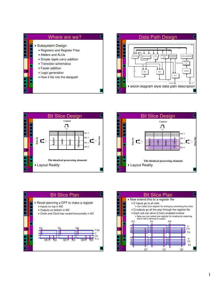
Where are we? Data Path Design � Subsystem Design � Registers and Register Files � Adders and ALUs � Simple ripple carry addition � Transistor schematics � Faster addition � Logic generation � How it fits into the datapath � Block-diagram style data path description Bit Slice Design Bit Slice Design Control Control Bit 3 Bit 3 Multiplexer Data-Out Bit 2 Multiplexer Data-Out Data-In Register Bit 2 Data-In Register Adder Shifter Adder Shifter Bit 1 Bit 1 Bit 0 Bit 0 Tile identical processing elements Tile identical processing elements � Layout Reality � Layout Reality Bit Slice Plan Bit Slice Plan � Now extend this to a register file � Recall planning a DFF to make a register � D inputs go to all cells � Inputs on top in M2 � Can select one register for writing by controlling the clock � Q outputs go all the way through the register file � Outputs on bottom in M2 � Each cell can drive Q from enabled inverter � Clock and Clock-bar routed horizontally in M1 � Now you can select one register for reading by selecting which cell is driving its output D2 D1 D0 C D2 D1 D0 Cb Vdd En C Cb Vss C Qb2 Q2 Qb1 Q1 Qb0 Q0 Cb En Q2 Q1 Q0 1
Bit Slice Plan Bit Slice Design En Cb Cb Cb En C En C En Cb C Control C Q0 Bit 3 D0 Multiplexer Data-Out Data-In Bit 2 Register Adder Shifter Q1 Bit 1 Bit 0 D1 Q2 Tile identical processing elements D2 Multi-Port Register Multi-Port Register Re1 Re0 Bit Slice Design Bit Slice Design Control Control Bit 3 Bit 3 Data-Out Data-Out Multiplexer Multiplexer Bit 2 Bit 2 Data-In Data-In Register Register Adder Adder Shifter Shifter Bit 1 Bit 1 Bit 0 Bit 0 Tile identical processing elements Tile identical processing elements � Where are power lines? Basic Comb � Where are power lines? scheme 2
Chip-Wide View of Power Chip-Wide View of Power � Power � Power Routing is a Routing is a global chip- global chip- wide issue wide issue � Here’s � Here’s another another approach approach � Note the � Note the Vdd and Vdd and Gnd pads Gnd pads � Global rings � Global rings with combs with combs for regions for regions of the chip of the chip Core power routing Core power routing Chip-Wide View of Power A Tweak on the Scheme � Another � Same basic view of the scheme same issue � But with no � Watch out internal for routing jumpers blockages! � Jumpers are restricted to outer loops 3
Adders Etc. Basic Addition: Full Adder A B � Check out Chapter 10 in your text Full Cin Cout adder Sum kill kill Boolean Equations A Direct Implementation A B Full Cin Cout adder Sum Fig 10.3 in your text… 32 transistors Use the Factored Equations Getting Rid of Inverters V D D Even C ell O dd C ell V DD B C i A A 3 B 3 A 1 B 1 A 0 B 0 A 2 B 2 A B A B C o, 2 C o ,3 C i ,0 C o ,0 C o ,1 C i B FA’ FA ’ FA’ FA ’ V DD A X C i C i A S S 0 S 2 S 1 S 3 C i A B B V DD A B C i A C o B Exploit Inversion Property Note: need 2 different types of cells 28 Transistors � Can improve performance by removing � Fully static, complex gate implementation inverters from carry chain 4
A Better Static Gate A Better Static Gate � Sometimes called a “mirror adder” � Combine gates and reuse subterms Mirror Adder Considerations Adder Layout � Examples •Feed the Carry-In to the inner inputs so the internal capacitance is already discharged from Weste •Make all transistors whose gates are connected to Cin and and carry logic minimum size – minimizes branching Eshraghian effort on critical path (carry out) � “Standard •Determine gate widths by Logical Effort – reduce effort from C to CoutB at the expense of Sum Cell” vs. •Use relatively large transistors on critical path so that “Datapath” stray wiring cap is a small fraction of overall cap � Definitely worth looking at carefully Datapath Layout Datapath Layout � A little tricky to figure out � You may not want to use this exact layout, but it might give you ideas � Start by identifying vdd and gnd paths � Think about rotating it counter clock wise � Think about a taller circuit that matches the bit-pitch of your register… 5
Example Datapath Layout Addition and Subtraction � Remember back to your logic design class � Add the two’s complement to subtract � Take two’s complement by inverting all the bits and adding one � Use the carry-in to add one A B Out � Use an XOR to invert or not 0 0 0 0 1 1 1 0 1 1 1 0 Two’s Complement Add/Sub Aside: XOR Gates � Slightly tricky gate, ~AB + A~B � Lots of different schematics… Another XOR gate Yet Another XOR Gate � Not too bad if you already have A, ~A, B, � DCVSL (section 6.2.3 in your text) ~B floating around � Differential Cascode Voltage Switch Logic � If not, you’ll need a couple inverters too… � Make sure that the combinational pull-down networks are complementary ~B ~A B ~A A B A ~B Out ~Out XNOR XOR B ~A ~B ~A Differential PDN2 PDN1 Inputs A ~B A B 6
DCVSL XOR/XNOR Another DCVSL Example Out ~Out Out ~Out D B ~B A ~D ~E ~B B E B C A ~A ~B ~A ~C � Generates both XOR/XNOR � Pull-down stacks must be complementary � Still static, but might be slower than others DCVSL Large XOR DCVSL Large XOR Four-input XOR Four-input XOR aka odd parity aka odd parity Out ~Out Out ~Out ~D D ~D D ~D D ~D D C ~C C ~C C ~C C ~C B ~B B ~B B ~B B ~B ~A ~A A A DCVSL Large XOR Transmission Gate XOR Four-input XOR aka odd parity Out ~Out ~D D ~D D C ~C C ~C � Tiny, clever circuit B ~B B ~B � If A is high, N1, P1 act like inverter � If A is low, B is passed to the output through ~A A transmission gate 7
Transmission Gate Adder Another Version P V DD C i V DD A P S Sum Generation A A P C i P A V DD B B A V DD P P Carry Generation C o C i C i C i A P Setup Yet Another Version An Example Layout… � Not the same style we’re used to seeing… More Pass Transistors Speeding Up Addition � Complementary Pass Transistor Logic � It all comes back to the carry circuit (CPL) � Ripple carry delay goes from low-order to high-order bit � Slightly faster, but more area � This determines the speed of the addition B B B C B C A B C B C S C out A � Many many ways to speed up the carry B C B C A calculation B C B C S C out B A Section 10.2.2 in your text B 8
Carry Lookahead Carry Lookahead � Restated: C i = G i + P i C (i-1) � C0 = G 0 + P 0 C in � C1 = G 1 + P 1 C 0 = G 1 + P 1 (G 0 + P 0 C in ) = G 1 + P 1 G 0 + P 1 P 0 C in Sum = P + Ci � C2 = G 2 + P 2 G 2 + P 2 P 1 G 0 + P 2 P 1 P 0 C in � C3 = G 3 + P 3 G 2 + P 3 P 2 G 1 + P 3 P 2 P 1 G 0 -1 + P 3 P 2 P 1 P 0 C in � Key is that the carry depends ONLY on A � Or C 3 = G 3 + P 3 (G 2 +P 2 ( G 1 + P 1 (G 0 + P 0 C in ))) and B, not the carry-in � Catch is that the gates have large fan-in Carry Lookahead Carry Lookahead Logic A 0 ,B 0 A 1 ,B 1 A N-1 ,B N-1 ... C i,0 P 0 C i,1 P 1 C i,N-1 P N-1 ... � The C equations get larger with each stage � Usually do lookahead in small blocks (I.e. 4) and the combine in a tree Fast Carry Lookahead Logic Another Version V DD G 3 G 2 G 1 G 0 Pseudo-nMOS C i,0 C o,3 Uses lots of current! P 0 P 1 P 2 P 3 9
Another View Another View A 4 B 4 A 3 B 3 A 2 B 2 A 1 B 1 C in 1: Bitwise PG logic G 4 P 4 G 3 P 3 G 2 P 2 G 1 P 1 G 0 P 0 2: Group PG logic G 3:0 G 2:0 G 1:0 G 0:0 C 3 C 2 C 1 C 0 3: Sum logic C 4 C out S 4 S 3 S 2 S 1 Ripple Carry Ripple Carry A 4 B 4 A 3 B 3 A 2 B 2 A 1 B 1 C in A 4 B 4 A 3 B 3 A 2 B 2 A 1 B 1 C in G 4 P 4 G 3 P 3 G 2 P 2 G 1 P 1 G 0 P 0 G 4 P 4 G 3 P 3 G 2 P 2 G 1 P 1 G 0 P 0 G 3:0 G 2:0 G 1:0 G 0:0 G 3:0 G 2:0 G 1:0 G 0:0 C 3 C 2 C 1 C 0 C 3 C 2 C 1 C 0 C 4 C 4 C out S 4 S 3 S 2 S 1 C out S 4 S 3 S 2 S 1 C 3 = G 3 + P 3 (G 2 +P 2 ( G 1 + P 1 (G 0 + P 0 C in ))) PG Diagram Notation Ripple Carry = + − + t t ( N 1) t t Bit Position ripple pg AO xor 15 14 13 12 11 10 9 8 7 6 5 4 3 2 1 0 Black cell Gray cell Buffer i:k k-1:j i:k k-1:j i:j i:j i:j i:j Delay G G i:k G i:k G P i:j P i:j G G i:k i:k i:j i:j G G k-1:j k-1:j P P P i:j i:j P i:j 15:0 14:0 13:0 12:0 11:0 10:0 9:0 8:0 7:0 6:0 5:0 4:0 3:0 2:0 1:0 0:0 k-1:j 10
Recommend
More recommend