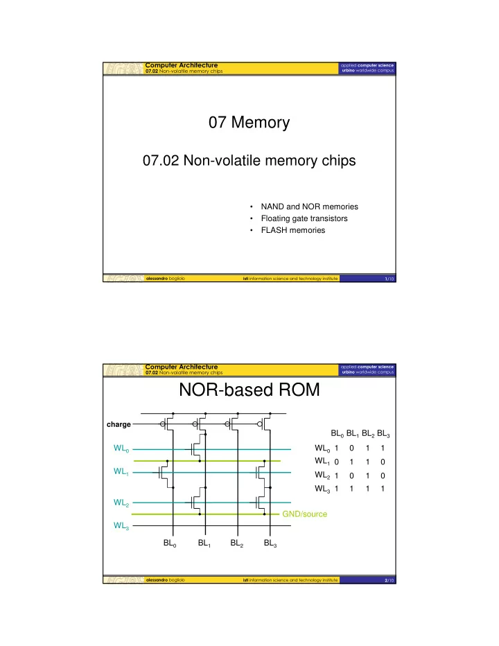
nor based rom
play

NOR-based ROM charge BL 0 BL 1 BL 2 BL 3 WL 0 WL 0 1 0 1 1 WL 1 - PDF document


  1. ��������������������� �������� ���������������� ������ ������������������������� ������ ���������������� 07 Memory 07.02 Non-volatile memory chips • NAND and NOR memories • Floating gate transistors • FLASH memories ���������� �������� ���� �������������������������������������������� � ��� ��������������������� �������� ���������������� ������ ������������������������� ������ ���������������� NOR-based ROM charge BL 0 BL 1 BL 2 BL 3 WL 0 WL 0 1 0 1 1 WL 1 0 1 1 0 WL 1 WL 2 1 0 1 0 WL 3 1 1 1 1 WL 2 GND/source WL 3 BL 0 BL 1 BL 2 BL 3 ���������� �������� ���� �������������������������������������������� � ���

  2. ��������������������� �������� ���������������� ������ ������������������������� ������ ���������������� NAND-based ROM charge BL 0 BL 1 BL 2 BL 3 BL 0 BL 1 BL 2 BL 3 WL 0 WL 0 0 1 0 0 WL 1 1 0 0 1 WL 1 WL 2 0 1 0 1 WL 2 WL 3 0 0 0 0 WL 3 ���������� �������� ���� �������������������������������������������� � ��� ��������������������� �������� ���������������� ������ ������������������������� ������ ���������������� Floating gate transistor Control gate Erasure (Fowler-Nordheim Floating gate - tunneling) Programming - n+ source n+ drain (F-N tunneling) - Programming (hot-electron injection) p-substrate bulk ���������� �������� ���� �������������������������������������������� � ���

  3. ��������������������� �������� ���������������� ������ ������������������������� ������ ���������������� Floating gate transistor (programming/writing) ∆ Q FG ∆ V = − T C FG V GS With positive Without charge With negative charge in the FG charge in the FG in the FG 0 0 0 1 1 1 Works like a transistor Works like a short circuit Works like an open line ���������� �������� ���� �������������������������������������������� � ��� ��������������������� �������� ���������������� ������ ������������������������� ������ ���������������� NOR-based flash memories • Read – Random access, like a ROM • Erase – F-N tunneling • Write (programming) – Hot-electron injection • Interface – Common flash interface • Applications – Execute in place ���������� �������� ���� �������������������������������������������� � ���

  4. ��������������������� �������� ���������������� ������ ������������������������� ������ ���������������� NAND-based flash memories • Read – Sequential • Erase – F-N tunneling (release) • Write (programming) – F-N tunneling (injection) • Interface – Like a block device – MMU required to support execute-in-place • Applications – File system ���������� �������� ���� �������������������������������������������� � ��� ��������������������� �������� ���������������� ������ ������������������������� ������ ���������������� Multi-level flash cells • Multi-level cell – Control the amount of charge in the floating gate – Sense the current level rather than the presence of current – Store 2 or more bits in a single cell • DiskOnChip – High storage capacity – Built-in file system – Built-in execute-in-place ���������� �������� ���� �������������������������������������������� � ���

  5. ��������������������� �������� ���������������� ������ ������������������������� ������ ���������������� DiskOnChip vs NOR vs NAND DiskOnChip NOR NAND Capacity 8MB-1024MB 1MB-32MB 16MB-512MB XIP (code execution) XIP boot block Yes None Performance Fast erase (3 msec) VERY SLOW erase (5 sec) Fast erase (3 msec) Fast write Slow write Fast write Fast read Fast read Fast read Reliability Extremely high: Standard: Low: Built-in EDC/ECC solves bit-flipping. Bit-flipping issues reported Requires 1-4 bit EDC/ECC due to bit-flipping issue. Bad block managed by TrueFFS. Less than 10% the life span of NAND. Requires bad-block management. Erase Cycles 100,000 - 1,000,000 10,000 - 100,000 100,000 - 1,000,000 Interface SRAM/NOR-like Full memory interface I/O only Access Method RND on code area, SEQ on data Random Sequential area. Ideal Usage Both data and code storage in any Code storage - limited capacity due to Data storage only - due to application that requires a file system. price in high capacity. May save limited complicated flash management. data as well. Code will usually not be stored in raw NAND flash. Examples Smartphones Simple home appliances PC Cards PDAs Embedded designs Compact Flash Point-Of-Sale Workstations Low-end set top boxes Secure Digital SCB/IPC Low-end mobile handsets MP3 players Digital Gateways PC BIOS chips Digital Cameras Telecom Equipment Set-Top Boxes Thin Clients Price Low High Low http://www.m-sys.com/site/en-US/Corporate/Technology/NANDandNOR_Flash_Technologies.htm ���������� �������� ���� �������������������������������������������� � ��� ��������������������� �������� ���������������� ������ ������������������������� ������ ���������������� Flash vs HDD • No random-access rewrite – Require complex built-in interfaces • Higher cost – NAND flashes have the lowest cost per bit • Limited number of erase-write cycles – Read-most memories • Much lower power consumption ���������� �������� ���� �������������������������������������������� �� ���

Download Presentation
Download Policy: The content available on the website is offered to you 'AS IS' for your personal information and use only. It cannot be commercialized, licensed, or distributed on other websites without prior consent from the author. To download a presentation, simply click this link. If you encounter any difficulties during the download process, it's possible that the publisher has removed the file from their server.

Recommend


More recommend