
SLIDE 1
1
Memory Hierarchy Design
Chapter 5 and Appendix C
1
Overview
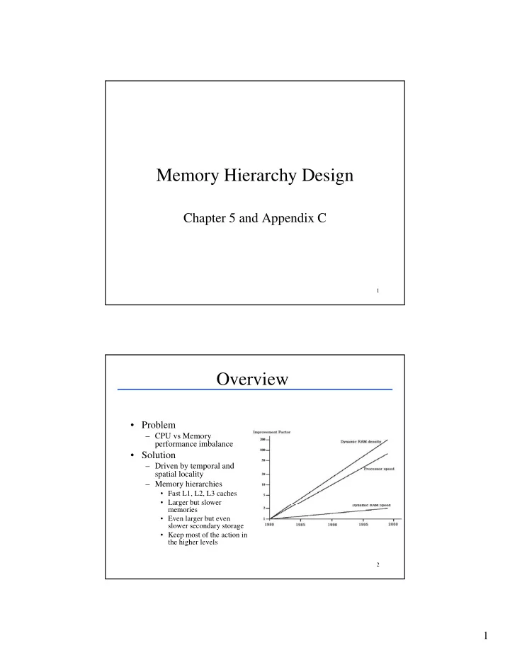
- Problem
– CPU vs Memory performance imbalance
- Solution
– Driven by temporal and spatial locality – Memory hierarchies
- Fast L1, L2, L3 caches
- Larger but slower
2
Larger but slower memories
- Even larger but even
slower secondary storage
- Keep most of the action in
the higher levels