
SLIDE 1
Sebastian Hofferberth, Igor Lesanovsky, Bettina Fischer, Thorsten Schumm, Jörg Schmiedmayer
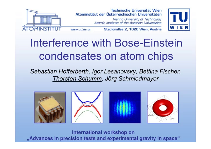
Interference with Bose-Einstein condensates on atom chips
International workshop on „Advances in precision tests and experimental gravity in space“