=$ High$ESR$ Aluminum$($$)$ High$Value$ Low$ESR$ Tantalum$($$$)$ - - PDF document

high esr aluminum high value low esr tantalum high value
SMART_READER_LITE
LIVE PREVIEW

=$ High$ESR$ Aluminum$($$)$ High$Value$ Low$ESR$ Tantalum$($$$)$ - - PDF document

Goals$ Learn$basic$PCB$crea=on$theory$ Learn$commands$for$naviga=ng$EAGLE$ ! Create$a$new$part,$place$it$in$a$schema=c,$and$route$it$


slide-1
SLIDE 1

!

Sam$DeBruin$ EECS$373$10/30/2014$
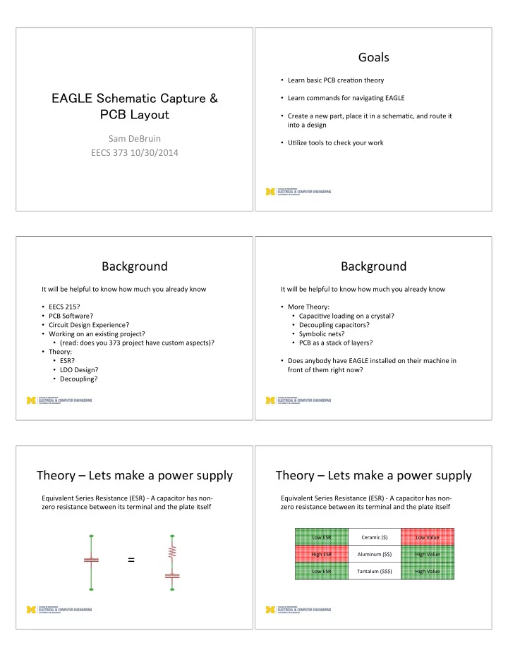
Goals$

  • Learn$basic$PCB$crea=on$theory$
  • Learn$commands$for$naviga=ng$EAGLE$
  • Create$a$new$part,$place$it$in$a$schema=c,$and$route$it$

into$a$design$

  • U=lize$tools$to$check$your$work$

Background$

It$will$be$helpful$to$know$how$much$you$already$know$

  • EECS$215?$
  • PCB$SoOware?$
  • Circuit$Design$Experience?$
  • Working$on$an$exis=ng$project?$
  • (read:$does$you$373$project$have$custom$aspects)?$
  • Theory:$
  • ESR?$
  • LDO$Design?$
  • Decoupling?$

Background$

It$will$be$helpful$to$know$how$much$you$already$know$

  • More$Theory:$
  • Capaci=ve$loading$on$a$crystal?$
  • Decoupling$capacitors?$
  • Symbolic$nets?$
  • PCB$as$a$stack$of$layers?$
  • Does$anybody$have$EAGLE$installed$on$their$machine$in$

front$of$them$right$now?$

Theory$–$Lets$make$a$power$supply$

Equivalent$Series$Resistance$(ESR)$\$A$capacitor$has$non\ zero$resistance$between$its$terminal$and$the$plate$itself$

=$

Theory$–$Lets$make$a$power$supply$

Equivalent$Series$Resistance$(ESR)$\$A$capacitor$has$non\ zero$resistance$between$its$terminal$and$the$plate$itself$

Low$ESR$ Ceramic$($)$ Low$Value$ High$ESR$ Aluminum$($$)$ High$Value$ Low$ESR$ Tantalum$($$$)$ High$Value$

slide-2
SLIDE 2

Theory$–$Lets$make$a$power$supply$

LDO$Design$–$simple$supply$and$easy$to$get$right,$but$ consider$ESR$

Low$ESR$requirement$means$use$at$least$one$ceramic$cap,$close$to$the$IC$

Theory$–$Signals$can$Interfere$

A$high$speed$digital$signal$in$a$wire$will$act$as$an$antenna$

Theory$–$Signals$can$Interfere$

And$will$induce$a$similar$signal$in$adjacent$wires$

Theory$–$Signals$can$Interfere$

Worse,$it$goes$both$ways!$

Theory$–$Signals$can$Interfere$

Worse,$it$goes$both$ways!$ Neither$signal$ is$usable$

Theory$–$Signals$can$Interfere$

If$the$antenna$analogy$doesn’t$work$for$you,$its$also$called$$ $ Capaci&ve)Coupling) ) An$implied$capacitor$between$the$lines,$and$a$capacitor$resists$changes$in$voltage$

slide-3
SLIDE 3

Theory$–$Signals$can$Interfere$

Either$way,$solve$it$with$a$ground$plane$(copper$poured$in\between$and$connected$to$GND):$ $ For$you$antenna$folks,$the$plane$is$a$faraday$cage$ $ For$you$capacitor$folks,$the$plane$is$dominated$by$two$separate$capacitors$ GND$Plane$

Theory$–$Decoupling$

Power$supplies$are$inherently$noisy,$microprocessors$and$other$ICs$cant$handle$that$ $ $ $ $ $ $ $ $ $ $ $ $ Microprocessor$App$Note$will$describe$decoupling$requirements,$loca=on$is$key!$ Typically$at$least$one$0.1uF$ceramic$for$every$power$pin$ $

Theory$–$Capaci=ve$Loading$

Capaci=ve$loads$are$used$to$temper$crystal$oscilla=ons$speeds$–$more$capacitance$ means$slower$oscilla=on$$ $ Both$the$crystal$and$the$microcontroller$are$expec=ng$a$certain$load$ $ $ $ $ $ $ $ $ $ This$is$voodoo$magic,$best$prac=ce$is$to$get$the$crystal$part$number$from$the$ microcontroller$datasheet,$and$use$the$capacitor$values$it$recommends$$ $ $ $ $ $

Theory$–$PCB$is$a$stack$of$layers$

Alterna=ng$metal$and$non\metal.$At$least$two$metal$layers,$or$many$more$ $ $ $ $ $ $ $ $ $ $ $ $ Vias$(plated$holes)$allow$signals$to$move$between$the$layers$ $ $ $ $ $

?! Circuit$Design$–$30,000$feet$

  • 1. What$is$the$circuit$supposed$to$do?$Where$will$power$

come$from?$What$are$the$form$factor$requirements?$ (concept)$

  • 2. Which$parts$are$need$to$be$included$to$realize$goals?$

(part$selec=on)$

  • 1. Do$you$have$libraries?$(part$crea=on)$
  • 3. How$does$it$all$connect?$(schema=c$capture$\$readable)$
  • 4. Where$does$it$all$go?$(PCB$layout$–$no$shorts)$
slide-4
SLIDE 4

EAGLE$\$Naviga=on$

  • Zoom$in/out$with$the$scroll$wheel$
  • Pan$by$pressing$&$holding$the$middle$mouse$buhon$
  • Mac$mul=touch$works$well$(two$finger$zoom,$three$

finger$pan,$etc)$

  • Otherwise$I$don’t$recommend$using$a$trackpad$

EAGLE$\$Commands$

  • Commands$can$be$launched$from$the$command$line$or$

from$buhons$ $ $

  • You$can$‘click’$from$the$command$line$too$
  • Only$interact$with$a$part$at$its$origin$
  • Exit$out$of$a$command$with$‘;’$or$$

$

Move$a$part$by$typing$‘move’$or$pressing$ When$running$‘wire’,$put$$a$wire$at$point$x=0.1”,$ y=0.1”$either$by$clicking$there$or$typing$(0.1$0.1)$

EAGLE$–$Schema=c$Capture$

  • Add$parts$using$‘add’$or$$
  • Copy$parts$using$‘copy’$or$
  • Move$using$‘move’$or$
  • Lots$of$other$commands$for$part$manipula=on$including$

‘rotate’,$‘delete’,$‘mirror’$to$be$explored$$$ $

EAGLE$–$Schema=c$Capture$

  • Once$you$have$added$parts,$connect$them$with$the$‘net’$

command$($$$$$)$

  • Net$allows$you$to$draw$wires$between$pins,$but$don’t$

use$‘wire’!!!$

  • Difference$lies$in$junc=ons$(‘junc’):$

$

vs$

EAGLE$–$Schema=c$Capture$

  • Un=l$this$point,$we$haven't$talked$about$libraries.$$
  • EAGLE$has$lots$of$preloaded$parts,$but$what$if$you$want$

a$different$part?$

  • Make$a$new$library!$

$

slide-5
SLIDE 5

EAGLE$–$Part$Crea=on$Interlude$

  • Making$parts$is$hard,$and$you$need$to$be$very$careful$
  • Like$the$pairing$of$the$schema=c$capture$and$the$PCB$

board$layout,$a$Part$has$mul=ple$components$

  • The$Symbol$is$what$goes$in$the$schema=c$
  • The$Package$is$what$goes$in$the$board$
  • The$Part$is$what$links$the$two.$$
  • The$part$is$where$you$map$Symbol$pins$to$

Package$pads.$Can$store$pn#$too.$$

EAGLE$–$Symbol$Crea=on$

  • Making$the$symbol$involves$placing$pins)and$connec=ng$

them$with$some$sort$of$an$outline$

  • Can$include$iden=fying$symbols$and$names$too$

)

  • This$is$the$readable$version$
  • Lots$of$flexibility$with$how$$

$this$looks,$depends$on$how$$ $you$want$to$see$it$

EAGLE$–$Package$Crea=on$

  • Making$the$package$involves$placing$pads)and)smds)
  • Can$s=ll$include$a$name$(called$a$Reference$Designator)$

)

  • This$is$the$physical$version$
  • Needs$to$be$exactly$the$size$

$and$dimensions$of$the$actual$ $part$

EAGLE$–$Part$Crea=on$

  • Part$is$what$you$actually$add$to$circuit$
  • Contains$both$symbol$and$package$
  • Primary$func=on$is$to$connect$

$pins$from$the$symbol$to$pads$ $and$smds$in$the$package$ $

  • Can$also$store$other$info$$

$(ahributes)$

EAGLE$–$Part$Crea=on$Interlude$

  • The$‘use’$command$allows$you$to$add$parts$from$your$

new$library$into$the$schema=c$

  • The$command$‘use$\*’$un\uses$all$the$default$libraries$if$

you$want$to$de\cluher$and$start$over$

  • EAGLE$scrip=ng$is$great$for$this$(outside$this$scope,$but$

follow$up$if$youre$interested).$$

EAGLE$–$Schema=c$Capture$

  • Other$useful$commands$in$the$schema=c$
  • ‘name’$$\$allows$you$to$assign$a$net’s$name.$Nets)

with)the)same)name)will)be)connected.$$

  • ‘label’$–$put$a$visual$label$showing$a$net’s$name$
  • ‘text’$–$put$text$down$in$the$schema=c$
  • ‘smash’$–$move$a$part’s$name$label$freely$
  • Don’t$forget$about$supply$net$symbols!$

Plus$lots$more!$

slide-6
SLIDE 6

EAGLE$–$Sch$\>$Brd$

  • Once$youre$(mostly)$done$type$‘board’$or$

And$the$board$is$made,$although$it$looks$prehy$funky$$

EAGLE$–$Board$Layout$

  • Layout$is$two$interweaving$but$separate$ac=ons:$
  • Placement$
  • Rou=ng$
  • Don’t$be$fooled$into$thinking$rou=ng$is$the$important$

step.$A$well$placed$board$routes$itself$(not$literally)$$

  • Place$based$on$1)$use$and$2)$circuit$

EAGLE$–$Rou=ng$

  • Once$youre$done$placing,$‘route’$
  • Those$yellow$lines$are$airwires$that$represent$routes\to\be$
  • Quick$=ps$
  • ‘route$<width>’$will$route$with$a$certain$width$trace$
  • Typing$‘layer$<l>’$while$rou=ng$will$place$a$via$and$

switch$to$that$layer$

  • Middle$click$while$rou=ng$also$switches$layer$
  • LeO$click$changes$angle$style$
  • Run$‘drc’$oOen$

EAGLE$–$Rou=ng$

  • Polygons$are$large$spaces$of$copper$“poured”$

$(remember$a$GND$pour$shields$traces)$ $

  • Polygons$on$the$board$are$ranked,$and$will$avoid$traces$
  • Generally$recommended$to$pour$top$and$bohom$with$GND$

EAGLE$–$Checking$Your$Work$

  • Run$‘erc’:$
  • Checks$for$inconsistencies$between$sch$and$brd$
  • Checks$for$minor$errors$in$sch$(single$pin$nets)$
  • Run$‘drc’:$(early$and$oOen!)$
  • Checks$for$viola=ons$of$the$design$rules$
  • Run$‘rats’:$(also$early$and$oOen!)$
  • Re\process$all$polygons$
  • Re\draw$all$airwires$to$shortest$paths$
  • Count$remaining$airwires$(displayed$in$bohom$leO)$
  • ‘rip$@;’$hides$polygons$aOerward$

EAGLE$–$Finishing$Up$

  • Board$house$(Advanced$Circuits,$Sunstone)$needs$Gerber$

files$$

  • Generate$these$using$the$CAM$processor$($$$$$)$
  • One$Gerber$file$for$each$layer$
  • Check$your$work$with$online$Gerber$viewer$tools$
  • Use$EAGLE$scripts$to$generate$dxf’s$for$stencils,$BOMs,$etc$

Seek$out$EAGLE$dru$and$CAM$job$files$from$the$board$house$

slide-7
SLIDE 7

PCB$Best$Prac=ces/Final$Checks$

  • Is$the$silkscreen$correct?$(Important$for$assembly)$
  • Is$the$silkscreen$readable?$
  • Are$connectors$obvious$in$the$silkscreen?$
  • Do$parts$have$part$numbers?$
  • Do$you$have$enough$test$points$(1.03mm)?$$
  • Can$everything$be$accessed$and$assembled?$
  • Are$LEDs$labeled?$
  • Is$there$a$power$LED$(alive$indicator)?$
  • I2c$addresses$non$conflic=ng,$CAN$stubs$short$
  • Name$&$date$&$version$number$in$the$silkscreen$

?!

MESH$has$tutorials$complete$with$sample$.sch,$.brd,$and$.lbr$files$